2 9.11. Disassembly of Front Panel Block ------------------- 34 9.12. Disassembly of Tuner Pack ---------------------------34 9.13. Disassembly of SMPS Unit ---------------------------- 35 9.14. Disassembly of AC IN P.C.B.--------------------------36 9.15. Disassembly of SMPS P.C.B. -------------------------38 9.16. Replacement of Switching Regulator IC (IC702)------------------------------------------------------ 39 9.17. Replacement of Diode (D702) ------------------------41 9.18. Replacement of Diode (D704) ------------------------43 9.19. Disassembly of Main P.C.B. ---------------------------45 9.20. Disassembly of Fan-------------------------------------- 48 9.21. Disassembly of AUX / HP P.C.B.---------------------48 9.22. Disassembly of Traverse Deck -----------------------49 9.23. Disassembly of Traverse Cover & Traverse Unit----------------------------------------------------------- 50 9.24. Disassembly of CD Servo P.C.B.---------------------51 9.25. Disassembly of D-Amp P.C.B. ------------------------52 9.26. Disassembly of Fan Unit (iPod) ----------------------52 9.27. Disassembly of FL P.C.B. ------------------------------53 9.28. Disassembly of iPod P.C.B.----------------------------54 9.29. Disassembly of Motor P.C.B.--------------------------58 9.30. Disassembly of Position SW P.C.B. -----------------59 9.31. Disassembly of iPod SW P.C.B.----------------------60 9.32. Disassembly of IR P.C.B.-------------------------------61 10 Service Position ------------------------------------------------- 62 10.1. Checking and Repairing Main P.C.B. ---------------62 10.2. Checking and Repairing D-Amp P.C.B.-------------68 10.3. Checking and Repairing FL P.C.B. ------------------68 10.4. Checking and Repairing CD Servo P.C.B.---------69 10.5. Checking and Repairing AC IN P.C.B.--------------69 10.6. Checking and Repairing SMPS P.C.B. -------------72 11 Voltage Measurement & Waveform Chart --------------- 74 11.1. CD SERVO P.C.B. ---------------------------------------74 11.2. D-AMP P.C.B. ---------------------------------------------75 11.3. FL P.C.B. ---------------------------------------------------75 11.4. MAIN P.C.B. (1/3) ----------------------------------------76 11.5. MAIN P.C.B. (2/3) ----------------------------------------77 11.6. MAIN P.C.B. (3/3) ----------------------------------------78 11.7. SMPS P.C.B. ----------------------------------------------78 11.8. Waveform Chart ------------------------------------------79 12 Illustration of IC’s, Transistors and Diodes ------------ 81 13 Overall Simplified Block -------------------------------------- 82 14 Block Diagram --------------------------------------------------- 85 14.1. CD SERVO BLOCK DIAGRAM ---------------------- 85 14.2. MAIN (1/2) / TUNER / iPod / FL / MOTOR BLOCK DIAGRAM--------------------------------------- 86 14.3. MAIN (2/2) / D-AMP BLOCK DIAGRAM ----------- 87 14.4. PANEL1/2 / AUX/HP / IR / SMPS / AC IN BLOCK DIAGRAM--------------------------------------- 88 15 Wiring Connection Diagram --------------------------------- 89 16 Schematic Diagram Notes ----------------------------------- 90 17 Schematic Diagram--------------------------------------------- 91 17.1. CD SERVO CIRCUIT ----------------------------------- 91 17.2. MAIN CIRCUIT (1/4) ------------------------------------ 92 17.3. MAIN CIRCUIT (2/4) ------------------------------------ 93 17.4. MAIN CIRCUIT (3/4) ------------------------------------ 94 17.5. MAIN CIRCUIT (4/4) ------------------------------------ 95 17.6. FL CIRCUIT, PANEL 1 CIRCUIT and PANEL 2 CIRCUIT ------------------------------------------------- 96 17.7. TUNER CIRCUIT, AUX/HP CIRCUIT, IR CIRCUIT, MOTOR CIRCUIT, POSITION SW CIRCUIT and iPod SW CIRCUIT-------------------- 97 17.8. iPod CIRCUIT and AC IN CIRCUIT----------------- 98 17.9. D-AMP CIRCUIT----------------------------------------- 99 17.10. SMPS CIRCUIT -----------------------------------------100 18 Printed Circuit Board----------------------------------------- 101 18.1. CD SERVO P.C.B.--------------------------------------101 18.2. MAIN P.C.B. (1/2)---------------------------------------102 18.3. MAIN P.C.B. (2/2)---------------------------------------103 18.4.TUNER P.C.B., FL P.C.B., PANEL 1 P.C.B., PANEL 2 P.C.B., AUX/HP P.C.B. and IR P.C.B. ------------------------------------------------------104 18.5. MOTOR P.C.B., POSITION SW P.C.B., iPod SW P.C.B., iPod P.C.B. and D-Amp P.C.B. ------105 18.6. SMPS P.C.B. and AC IN P.C.B.---------------------106 19 Terminal Function of IC’s ----------------------------------- 107 19.1. IC801 (RFKWMAHC3-S) MICRO PROCESSOR IC --------------------------------------- 107 19.2. IC7001 (MN6627954AMA) IC SERVO PROCESSOR -------------------------------------------108 19.3. IC7002 (BA5948FPE2) IC 4CH Drive -------------109 20 Exploded View and Replacement Parts List ---------- 110 20.1. Exploded View and Mechanical replacement Parts List-------------------------------------------------- 110 20.2. Electrical Replacement Parts List ------------------ 116 Downloaded from www.Manualslib.com manuals search engine
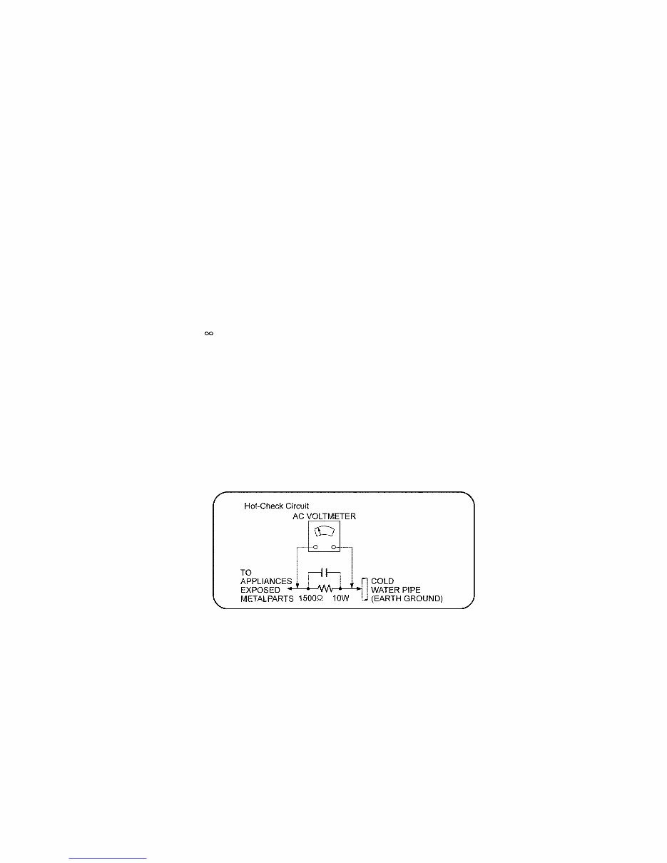
3 1 Safety Precautions 1.1. General Guidelines 1. When servicing, observe the original lead dress. If a short circuit is found, replace all parts which have been overheated or damaged by the short circuit. 2. After servicing, see to it that all the protective devices such as insulation barriers, insulation papers shields are properly installed. 3. After servicing, carry out the following leakage current checks to prevent the customer from being exposed to shock hazards. (This “Safety Precaution” is applied only in U.S.A.) 1. Before servicing, unplug the power cord to prevent an electric shock. 2. When replacing parts, use only manufacturer’s recommended components for safety. 3. Check the condition of the power cord. Replace if wear or damage is evident. 4. After servicing, be sure to restore the lead dress, insulation barriers, insulation papers, shields, etc. 5. Before returning the serviced equipment to the customer, be sure to make the following insulation resistance test to prevent the customer from being exposed to a shock hazard. 1.1.1. Leakage Current Cold Check 1. Unplug the AC cord and connect a jumper between the two prongs on the plug. 2. measure the resistance value, with an ohmmeter between the jumpered AC plug and each exposed metallic cabinet part on the equipment such as screwheads, connectors, control shafts, etc. When the exposed metallic part has a return path to the chassis, the reading should be between 1MΩ and 5.2MΩ. When the exposed metal does not have a return path to the chas- sis, the reading must be 1.1.2. Leakage Current Hot Check 1. Plug the AC cord directly into the AC outlet. Do not use an isolation transformer for this check. 2. Connect a 1.5kΩ, 10 watts resistor, in parallel with a 0.15μF capacitors, between each exposed metallic part on the set and a good earth ground such as a water pipe, as shown in Figure 1. 3. Use an AC voltmeter, with 1000 ohms/volt or more sensitivity, to measure the potential across the resistor. 4. Check each exposed metallic part, and measure the voltage at each point. 5. Reverse the AC plug in the AC outlet and repeat each of the above measurements. 6. The potential at any point should not exceed 0.75 volts RMS. A leakage current tester (Simpson Model 229 or equivalent) may be used to make the hot checks, leakage current must not exceed 1/2 milliamp. In case a measurement is outside of the limits specified, there is a possibility of a shock hazard, and the equipment should be repaired and rechecked before it is returned to the customer. Figure. 1 Downloaded from www.Manualslib.com manuals search engine
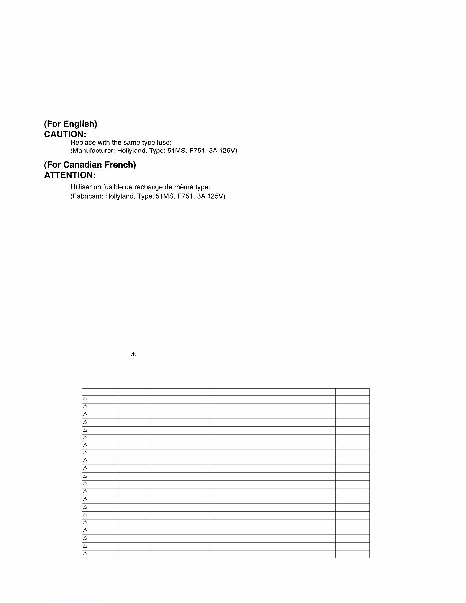
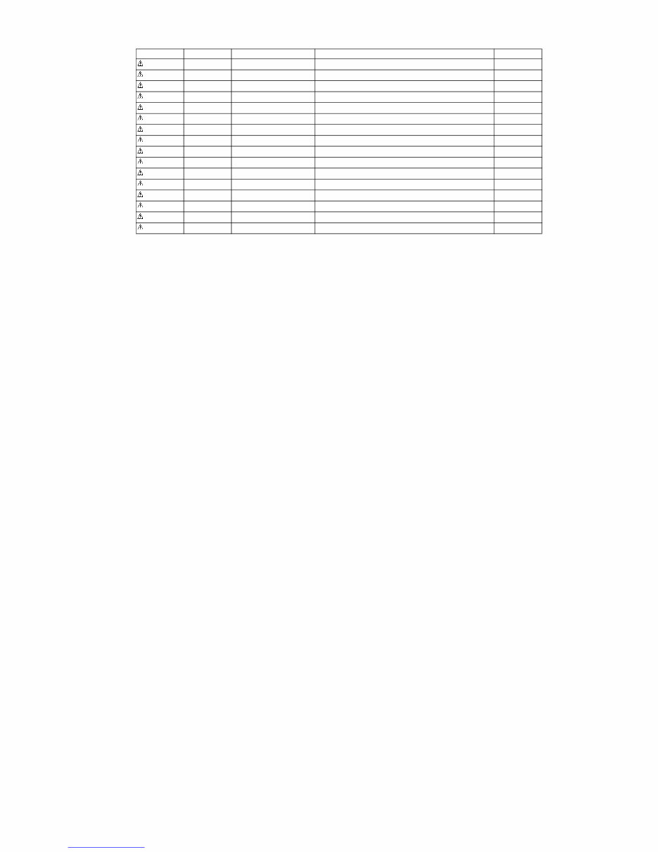
4 1.2. Before Repair and Adjustment Disconnect AC power, discharge unit AC Capacitors as such C702, C710, C725, C727, C728 and C730 through a 10W, 1W resistor to ground. Caution : DO NOT SHORT-CIRCUIT DIRECTLY (with a screwdriver blade, for instance), as this may destroy solid state devices. After repairs are completed, restore power gradually using a variac, to avoid overcurrent. • Current consumption at AC 120V, at 60Hz in NO SIGNAL mode (at volume min in FM Tuner mode) should be ~250 mA. 1.3. Caution For Fuse Replacement 1.4. Protection Circuitry The protection circuitry may have operated if either of the following conditions are noticed: • No sound is heard when the power is turned on. • Sound stops during a performance. The function of this circuitry is to prevent circuitry damage if, for example, the positive and negative speaker connection wires are "shorted", or if speaker systems with an impedance less than the indicated rated impedance of the amplifier are used. If this occurs, follow the procedure outlines below: 1. Turn off the power. 2. Determine the cause of the problem and correct it. 3. Turn on the power once again after one minute. Note: When the protection circuitry functions, the unit will not operate unless the power is first turned off and then on again. 1.5. Safety Part Information Safety Parts List: There are special components used in this equipment which are important for safety. These parts are marked by in the Schematic Diagrams, Exploded View & Replacement Parts List. It is essential that these critical parts should be replaced with manufacturer’s specified parts to prevent shock, fire or other hazards. Do not modify the original design without permission of manufacturer. Table 1 Safety Ref. No. Part No. Part Name & Description Remarks 6 REXX0746-1 RED WIRE (AC INLET-SMPS) 7 REXX0747-1 BLACK WIRE (AC INLET-SMPS) 9 REXX0752-1 BLUE WIRE (AC INLET-SMPS) 30 RGNX0850C-1 NAME PLATE PC 30 RGNX0850H-1 NAME PLATE P 101 REXX0771 WHITE WIRE (JW708) 102 REXX0772 BROWN WIRE (JW707) 300 RAE0165T-V TRAVERSE ASS’Y (RTL) A2 K2CB2CB00021 AC CORD A3 RQTX0250-1P O/I BOOK (En) A3 RQTX0251-1C O/I BOOK (Cf) PC A3 RQTX0254-1M O/I BOOK (Sp) P L702 G0B103G00015 LINE FILTER L703 G0B103G00015 LINE FILTER L751 ELF15N035AN LINE FILTER T581 G4D1A0000117 MAIN TRANSFORMER T701 G4DYA0000139 SUB TRANSFORMER T751 ETS19AB221AG SWITCHING TRANSFORMER Z752 ERZVA5Z471 ZNR PC701 B3PBA0000454 PHOTO COUPLER PC751 B3PBA0000454 PHOTO COUPLER Downloaded from www.Manualslib.com manuals search engine
6 2 Warning 2.1. Prevention of Electro Static Discharge (ESD) to Electrostatically Sensi- tive (ES) Devices Some semiconductor (solid state) devices can be damaged easily by static electricity. Such components commonly are called Elec- trostatically Sensitive (ES) Devices. Examples of typical ES devices are integrated circuits and some field-effect transistors and semiconductor “chip” components. The following techniques should be used to help reduce the incidence of component damage caused by electrostatic discharge (ESD). 1. Immediately before handling any semiconductor component or semiconductor-equiped assembly, drain off any ESD on your body by touching a known earth ground. Alternatively, obtain and wear a commercially available discharging ESD wrist strap, which should be removed for potential shock reasons prior to applying power to the unit under test. 2. After removing an electrical assembly equiped with ES devices, place the assembly on a conductive surface such as alumin- ium foil, to prevent electrostatic charge build up or exposure of the assembly. 3. Use only a grounded-tip soldering iron to solder or unsolder ES devices. 4. Use only an anti-static solder remover device. Some solder removal devices not classified as “anti-static (ESD protected)” can generate electrical charge sufficient to damage ES devices. 5. Do not use freon-propelled chemicals. These can generate electrical charges sufficient to damage ES devices. 6. Do not remove a replacement ES device from its protective package until immediately before you are ready to install it. (Most replacement ES devices are packaged with leads electrically shorted together by conductive foam, aluminium foil or compara- ble conductive material). 7. Immediately before removing the protective material from the leads of a replacement ES device, touch the protective material to the chassis or circuit assembly into which the device will be installed. Caution : Be sure no power is applied to the chassis or circuit, and observe all other safety precautions. 8. Minimize bodily motions when handling unpackaged replacement ES devices. (Otherwise harmless motion such as the brushing together of your clothes fabric or the lifting of your foot from a carpeted floor can generate static electricity (ESD) suf- ficient to damage an ES device). Downloaded from www.Manualslib.com manuals search engine
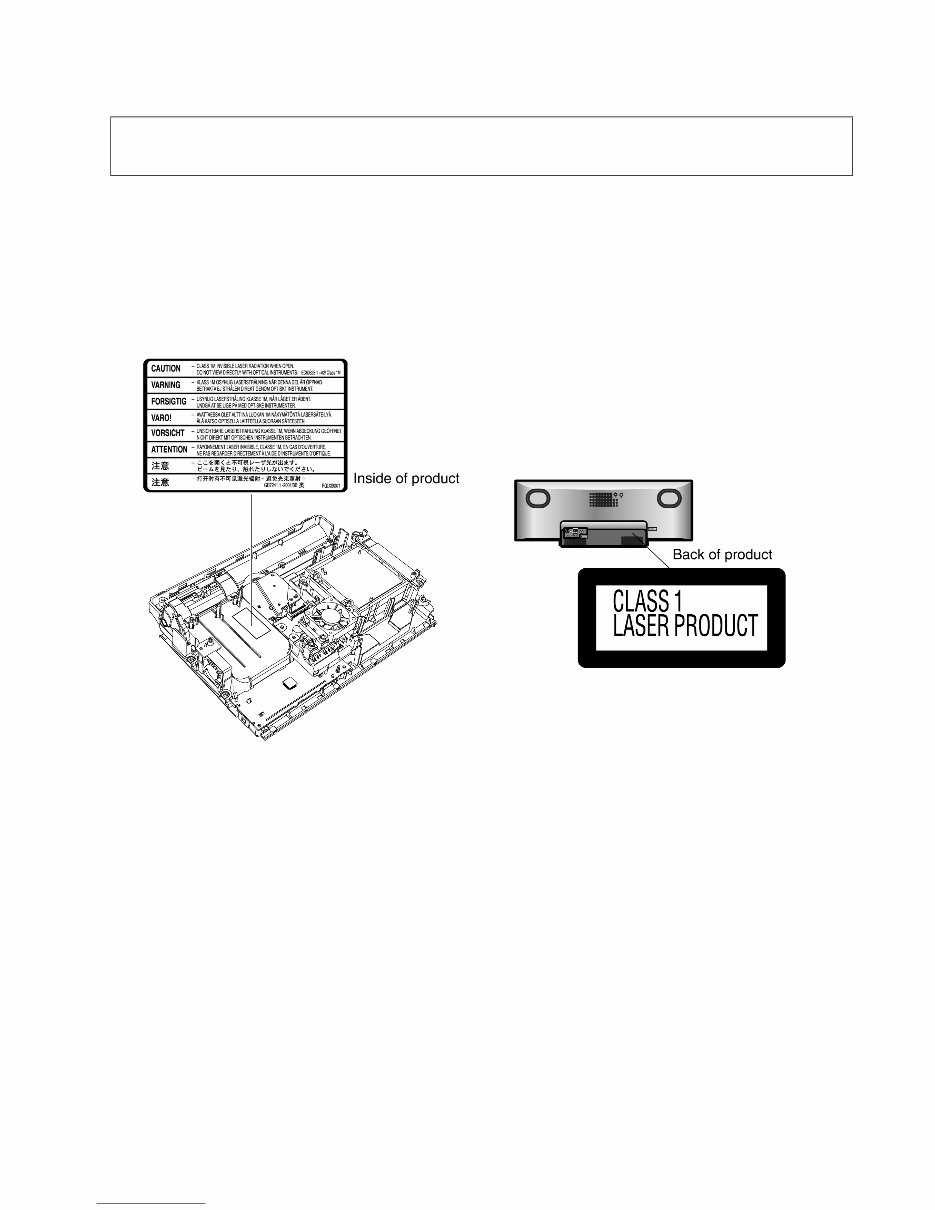
7 2.2. Precaution of Laser Diode Caution: This product utilizes a laser diode with the unit turned "on", invisible laser radiation is emitted from the pickup lens. Wavelength: 795 nm (CD) Maximum output radiation power from pickup: 100 μW/VDE Laser radiation from the pickup unit is safety level, but be sure the followings: 1. Do not disassemble the pickup unit, since radiation from exposed laser diode is dangerous. 2. Do not adjust the variable resistor on the pickup unit. It was already adjusted. 3. Do not look at the focus lens using optical instruments. 4. Recommend not to look at pickup lens for a long time. CAUTION! THIS PRODUCT UTILIZES A LASER. USE OF CONTROLS OR ADJUSTMENTS OR PERFORMANCE OF PROCEDURES OTHER THAN THOSE SPECIFIED HEREIN MAY RESULT IN HAZARDOUS RADIATION EXPOSURE. Downloaded from www.Manualslib.com manuals search engine
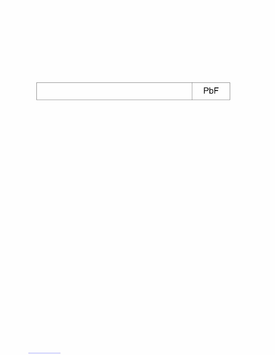
8 2.3. Service caution based on Legal restrictions 2.3.1. General description about Lead Free Solder (PbF) The lead free solder has been used in the mounting process of all electrical components on the printed circuit boards used for this equipment in considering the globally environmental conservation. The normal solder is the alloy of tin (Sn) and lead (Pb). On the other hand, the lead free solder is the alloy mainly consists of tin (Sn), silver (Ag) and Copper (Cu), and the melting point of the lead free solder is higher approx.30 degrees C (86°F) more than that of the normal solder. Definition of PCB Lead Free Solder being used Service caution for repair work using Lead Free Solder (PbF) • The lead free solder has to be used when repairing the equipment for which the lead free solder is used. (Definition: The letter of “PbF” is printed on the PCB using the lead free solder.) • To put lead free solder, it should be well molten and mixed with the original lead free solder. • Remove the remaining lead free solder on the PCB cleanly for soldering of the new IC. • Since the melting point of the lead free solder is higher than that of the normal lead solder, it takes the longer time to melt the lead free solder. • Use the soldering iron (more than 70W) equipped with the temperature control after setting the temperature at 350±30 degrees C (662±86°F). Recommended Lead Free Solder (Service Parts Route.) • The following 3 types of lead free solder are available through the service parts route. RFKZ03D01K-----------(0.3mm 100g Reel) RFKZ06D01K-----------(0.6mm 100g Reel) RFKZ10D01K-----------(1.0mm 100g Reel) Note * Ingredient: Tin (Sn), 96.5%, Silver (Ag) 3.0%, Copper (Cu) 0.5%, Cobalt (Co) / Germanium (Ge) 0.1 to 0.3% The letter of “PbF” is printed either foil side or components side on the PCB using the lead free solder. (See right figure) Downloaded from www.Manualslib.com manuals search engine
9 3 Service Navigation 3.1. Service Information This service manual contains technical information which will allow service perssonnel’s to understand and service this model. Please place orders using the parts list and not the drawing reference numbers. If the circuit is changed or modified, this information will be followed by supplement service manual to be filed with original service manual. 1. Micro-processor: • Micro-processor IC, (IC801) is supplied as assembled part (RFKWMAHC3-S). Downloaded from www.Manualslib.com manuals search engine
10 4 Specifications Amplifier Section RMS Output Power Stereo Mode Front Ch (both ch driven) 20 W per channel (6 Ω), 1 kHz, 10 % THD Phone jack Terminal Stereo, 3.5 mm jack Output level (CD, 1 kHz, -20 dB) max. 1.18 mW +1.18 mW, 32 Ω Aux (Rear) Sensitivity Normal level 630 mV, 12.4 kΩ High level 630 mV, 12.4 kΩ Terminal Stereo, 3.5 mm jack Tuner Section Preset memory FM 30 stations AM 15 stations Frequency Modulation (FM) Frequency range 87.9 MHz to 107.9 MHz (200 kHz step) 87.5 MHz to 108.0 MHz (100 kHz step) Antenna terminals 75 Ω (unbalanced) Amplitude Modulation (AM) Frequency range 520 kHz to 1710 kHz (10 kHz step) Disc Section Disc played [8 cm or 12 cm] (1) CD-Audio (CD-DA) (2) CD-R/RW (CD-DA, MP3) (3) MP3 * MPEG-1 Layer 3, MPEG-2 Layer 3 Pick up (CD) Wavelength 795 nm Laser power CLASS 1 Audio output (Disc) Number of channels FL, FR, 2 channel Audio performance (CD-Audio) Frequency response 4 Hz to 20 kHz S/N ratio 95 dB Dynamic range 93 dB Total harmonic distortion 0.005 % Speaker Section Type 1 way, 1 speaker system (Bass reflex) Speaker unit(s) Full range 6.5 cm Cone type Impedance 6 Ω Input power (IEC) 30 W (Max) Output sound pressure 79 dB/W (1.0m) Frequency range 55 Hz to 25 kHz (-16 dB) 90 Hz to 22 kHz (-10 dB) General Power supply AC 120 V, 60 Hz Power consumption 28 W Dimensions (W x H x D) 500 mm x 195 mm x 102.5 mm (19 11/16" x 7 11/16" x 4 1/16") [D = 69 mm (2 3/4") minimum] Mass Approx. 3 kg (6.6 lbs) Operating temperature range 0°C to +35°C (+32 °F to +95 °F) Operating humidity range 35% to 80 % RH (no condensa- tion) Power consumption in standby mode 0.2 W (approx) Notes : 1. Specifications are subject to change without notices. Mass and dimensions are approximate. 2. Total harmonic distortion is measured by the digital spectrum ana- lyzer. Downloaded from www.Manualslib.com manuals search engine
This service and repair manual is an essential resource for anyone looking to troubleshoot and repair their Panasonic SC HC3 stereo system. It is utilized by Official Certified Panasonic Technicians and provides comprehensive guidance on various aspects of the device.
Key features of this manual include:
Safety & Precautions
Product Specifications
Self Diagnostics
Disassembly & Reassembly
Adjustments
Troubleshooting
Voltage Measurement & Waveform Chart
Maintenance
Schematic Diagram
Block Diagram
Circuit Boards
Wiring Diagrams
Exploded Views
Replacement parts list
This manual covers ALL worldwide SC-HC3 models, including SC-HC3P and SC-HC3PC. It is highly detailed and includes illustrated pictures and step-by-step instructions for effective repair and servicing of the device.
It is important to note that this is the OFFICIAL service and repair manual in PDF format, ensuring the highest resolution for quality printing. Upon payment, you will have instant access to the manual without any shipping fees, allowing you to commence repairs promptly.