

© 2007 Matsushita Electric Industrial Co., Ltd. All
rights reserved. Unauthorized copying and
distribution is a violation of law.
Vol. 1
Colour
(S).......................Silver Type
(K).......................Black Type
DVD Recorder
ORDER NO.DSD0704009CE
Model No.
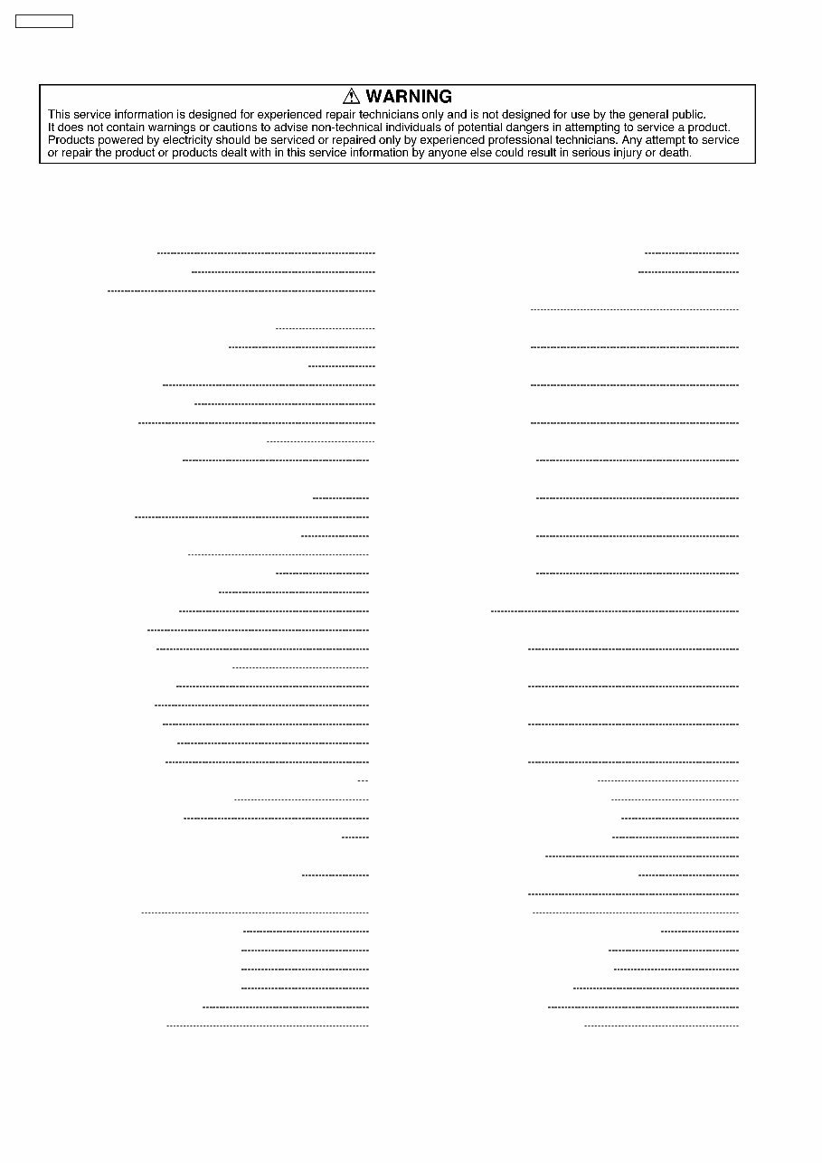
1 Safety Precaution 3
1.1. General guidelines 3
2 Warning 4
2.1. Prevention of Electrostatic Discharge (ESD) to
Electrostatic Sensitive (ES) Devices 4
2.2. Precaution of Laser Diode 5
2.3. Service caution based on legal restrictions 6
3 Service Navigation 7
3.1. Service Information 7
4 Specifications 8
5 Location of Controls and Components 9
6 Operation Instructions 10
6.1. Taking out the Disc from DVD-Drive Unit when the Disc
cannot be ejected by OPEN/CLOSE button 10
7 Service Mode 13
7.1. Self-Diagnosis and Special Mode Setting 13
8 Service Fixture & Tools 22
9 Disassembly and Assembly Instructions 23
9.1. Disassembly Flow Chart 23
9.2. P.C.B. Positions 24
9.3. Top Case 25
9.4. Front Panel 25
9.5. RAM/Digital P.C.B. Module 26
9.6. DV Jack P.C.B. 27
9.7. Rear Panel 28
9.8. HDMI P.C.B. 28
9.9. Backend P.C.B. 28
9.10. Power P.C.B. 29
9.11. Main P.C.B., Front Jack P.C.B. and Front (L) P.C.B. 29
10 Measurements and Adjustments 30
10.1. Service Positions 30
10.2. Notice after replacing RAM/Digital P.C.B. Module 33
10.3. When the unit does not operate normally after replacing
the Timer Microprocessor or Main P.C.B. 33
10.4. Standard Inspection Specifications after Making Repairs 34
11 Block Diagram 35
11.1. Power Supply Block Diagram 35
11.2. Analog Video Block Diagram 37
11.3. Analog Audio Block Diagram 38
11.4. Analog Timer Block Diagram 39
11.5. HDMI Block Diagram 40
12 Schematic Diagram 41
12.1. Interconnection Schematic Diagram 41
12.2. Power Supply Schematic Diagram 42
12.3. Main Net (1/4) Section (Main P.C.B. (1/4)) Schematic
Diagram (M) 43
12.4. Main Net (2/4) Section (Main P.C.B. (1/4)) Schematic
Diagram (M) 44
12.5. Main Net (3/4) Section (Main P.C.B. (1/4)) Schematic
Diagram (M) 45
12.6. Main Net (4/4) Section (Main P.C.B. (1/4)) Schematic
Diagram (M) 46
12.7. AV I/O (1/4) Section (Main P.C.B. (2/4)) Schematic
Diagram (AV) 48
12.8. AV I/O (2/4) Section (Main P.C.B. (2/4)) Schematic
Diagram (AV) 49
12.9. AV I/O (3/4) Section (Main P.C.B. (2/4)) Schematic
Diagram (AV) 50
12.10. AV I/O (4/4) Section (Main P.C.B. (2/4)) Schematic
Diagram (AV) 51
12.11. Tuner Section (Main P.C.B. (3/4)) Schematic Diagram
(TU) 53
12.12. Timer (1/4) Section (Main P.C.B. (4/4)) Schematic
Diagram (T) 54
12.13. Timer (2/4) Section (Main P.C.B. (4/4)) Schematic
Diagram (T) 55
12.14. Timer (3/4) Section (Main P.C.B. (4/4)) Schematic
Diagram (T) 56
12.15. Timer (4/4) Section (Main P.C.B. (4/4)) Schematic
Diagram (T) 57
12.16. HDMI Schematic Diagram 58
12.17. DV Jack Schematic Diagram 59
12.18. Front Jack Schematic Diagram 59
12.19. Front (L) Schematic Diagram 59
13 Printed Circuit Board 61
13.1. Power P.C.B. and DV Jack P.C.B. 61
13.2. Main P.C.B. 62
13.3. HDMI P.C.B. 67
13.4. Front Jack P.C.B. and Front (L) P.C.B. 68
14 Appendix for Schematic Diagram 69
14.1. Voltage and Waveform Chart 69
15 Parts and Exploded Views 76
15.1. Exploded Views 76
15.2. Replacement Parts List 78
CONTENTS
Page Page
2
DMR-EZ27EB
1.1.1. Leakage current cold check
1. Unplug the AC cord and connect a jumper between the two
prongs on the plug.
2. Measure the resistance value, with an ohmmeter, between
the jumpered AC plug and each exposed metallic cabinet
part on the equipment such as screwheads, connectors,
control shafts, etc. When the exposed metallic part has a
return path to the chassis, the reading should be between
1M and 5.2M.
When the exposed metal does not have a return path to the
chassis, the reading must be .
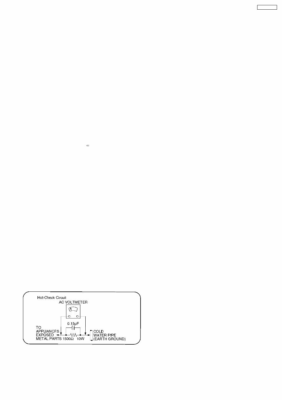
1.1.2. Leakage current hot check
(See Figure 1 .)
1. Plug the AC cord directly into the AC outlet. Do not use an
isolation transformer for this check.
2. Connect a 1.5k, 10 watts resistor, in parallel with a 0.15μF
capacitors, between each exposed metallic part on the set
and a good earth ground such as a water pipe, as shown in
Figure 1.
3. Use an AC voltmeter, with 1000 ohms/volt or more
sensitivity, to measure the potential across the resistor.
4. Check each exposed metallic part, and measure the
voltage at each point.
5. Reverse the AC plug in the AC outlet and repeat each of the
above measurements.
6. The potential at any point should not exceed 0.75 volts
RMS. A leakage current tester (Simpson Model 229 or
equivalent) may be used to make the hot checks, leakage
current must not exceed 1/2 milliampere. In case a
measurement is outside of the limits specified, there is a
possibility of a shock hazard, and the equipment should be
repaired and rechecked before it is returned to the
customer.
Figure 1
1 Safety Precaution
1.1. General guidelines
1. When servicing, observe the original lead dress. If a short circuit is found, replace all parts which have been overheated or
damaged by the short circuit.
2. After servicing, see to it that all the protective devices such as insulation barriers, insulation papers shields are properly
installed.
3. After servicing, make the following leakage current checks to prevent the customer from being exposed to shock hazards.
3
DMR-EZ27EB
2 Warning
2.1. Prevention of Electrostatic Discharge (ESD) to Electrostatic Sensitive
(ES) Devices
Some semiconductor (solid state) devices can be damaged easily by static electricity. Such components commonly are called
Electrostatic Sensitive (ES) Devices. Examples of typical ES devices are integrated circuits and some field-effect transistor-sand
semiconductor "chip" components. The following techniques should be used to help reduce the incidence of component damage
caused by electrostatic discharge (ESD).
1. Immediately before handling any semiconductor component or semiconductor-equipped assembly, drain off any ESD on your
body by touching a known earth ground. Alternatively, obtain and wear a commercially available discharging ESD wrist strap,
which should be removed for potential shock reasons prior to applying power to the unit under test.
2. After removing an electrical assembly equipped with ES devices, place the assembly on a conductive surface such as
aluminum foil, to prevent electrostatic charge buildup or exposure of the assembly.
3. Use only a grounded-tip soldering iron to solder or unsolder ES devices.
4. Use only an anti-static solder removal device. Some solder removal devices not classified as "anti-static (ESD protected)" can
generate electrical charge sufficient to damage ES devices.
5. Do not use freon-propelled chemicals. These can generate electrical charges sufficient to damage ES devices.
6. Do not remove a replacement ES device from its protective package until immediately before you are ready to install it. (Most
replacement ES devices are packaged with leads electrically shorted together by conductive foam, aluminum foil or comparable
conductive material).
7. Immediately before removing the protective material from the leads of a replacement ES device, touch the protective material
to the chassis or circuit assembly into which the device will be installed.
Caution
Be sure no power is applied to the chassis or circuit, and observe all other safety precautions.
8. Minimize bodily motions when handling unpackaged replacement ES devices. (Otherwise harmless motion such as the
brushing together of your clothes fabric or the lifting of your foot from a carpeted floor can generate static electricity sufficient
to damage an ES device).
4
DMR-EZ27EB
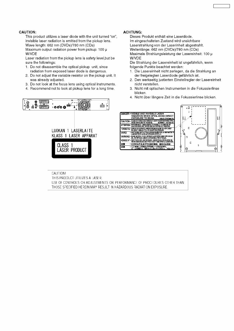
2.2. Precaution of Laser Diode
5
DMR-EZ27EB

2.3. Service caution based on legal restrictions
2.3.1. General description about Lead Free Solder (PbF)
The lead free solder has been used in the mounting process of all electrical components on the printed circuit boards used for this
equipment in considering the globally environmental conservation.
The normal solder is the alloy of tin (Sn) and lead (Pb). On the other hand, the lead free solder is the alloy mainly consists of tin
(Sn), silver (Ag) and Copper (Cu), and the melting point of the lead free solder is higher approx.30 degrees C (86°F) more than that
of the normal solder.
Definition of PCB Lead Free Solder being used
The letter of “PbF” is printed either foil side or components side on the PCB using the lead free solder.
(See right figure)
Service caution for repair work using Lead Free Solder (PbF)
The lead free solder has to be used when repairing the equipment for which the lead free solder is used.
(Definition: The letter of “PbF” is printed on the PCB using the lead free solder.)
To put lead free solder, it should be well molten and mixed with the original lead free solder.
Remove the remaining lead free solder on the PCB cleanly for soldering of the new IC.
Since the melting point of the lead free solder is higher than that of the normal lead solder, it takes the longer time to melt
the lead free solder.
Use the soldering iron (more than 70W) equipped with the temperature control after setting the temperature at 350±30
degrees C (662±86°F).
Recommended Lead Free Solder (Service Parts Route.)
The following 3 types of lead free solder are available through the service parts route.
RFKZ03D01K-----------(0.3mm 100g Reel)
RFKZ06D01K-----------(0.6mm 100g Reel)
RFKZ10D01K-----------(1.0mm 100g Reel)
Note
* Ingredient: tin (Sn), 96.5%, silver (Ag) 3.0%, Copper (Cu) 0.5%, Cobalt (Co) / Germanium (Ge) 0.1 to 0.3%
6
DMR-EZ27EB
3 Service Navigation
3.1. Service Information
7
DMR-EZ27EB
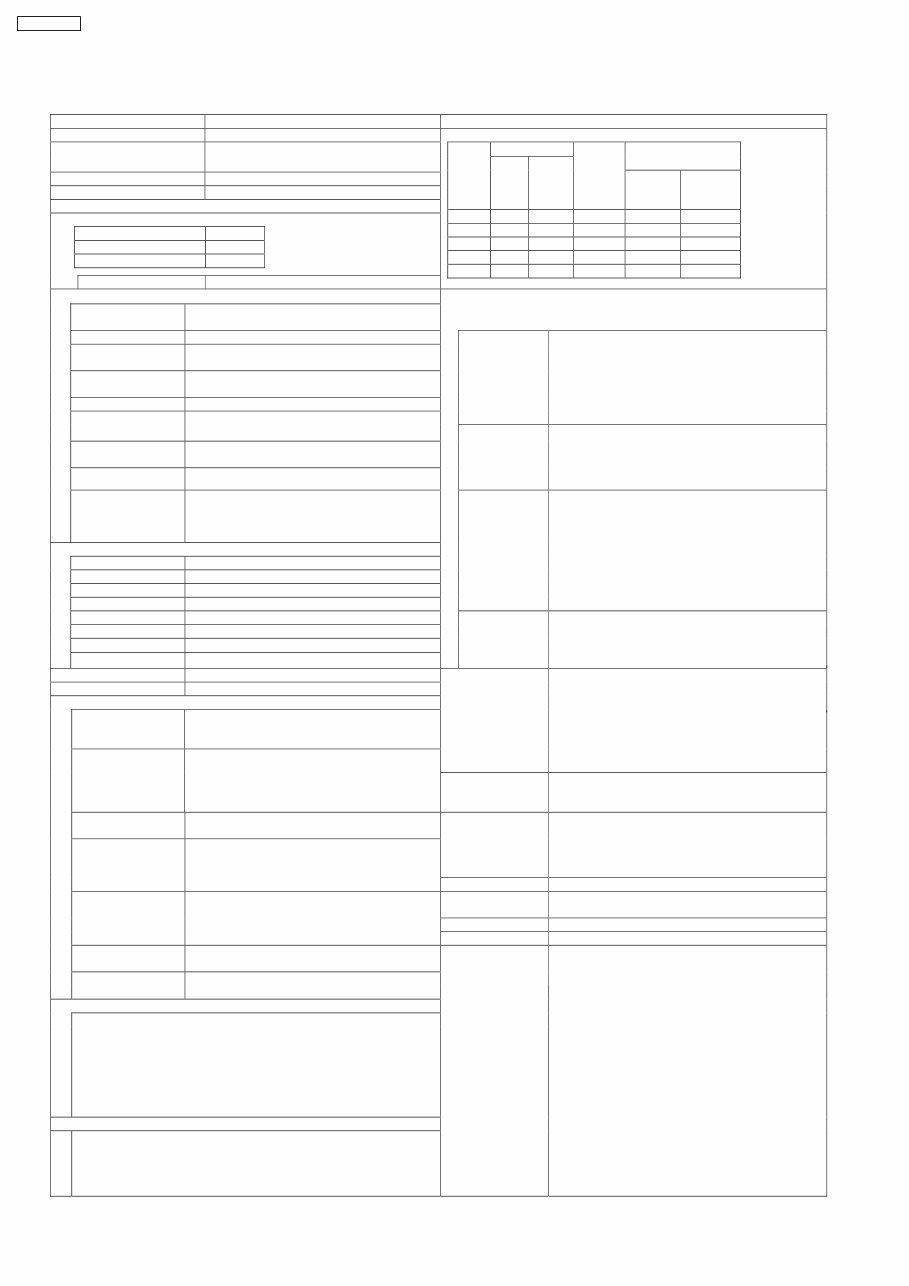
4 Specifications
Power supply: AC220 – 240V 50Hz Recording time
Power consumption: Approx. 25W
Power consumption in standby
mode:
Approx. 2W (Power save mode)
Approx. 15W (Quick start mode)
Operating temperature: 5 ºC - 40 ºC
Operating humidity range: 10% - 80%RH (no condensation)
Television system
Tuner system: DVB-T
Channel Coverage: UK
UHF: 21-68
RF Converter output: Not provided
Approx.
DVD-RAM DVD-R DL, +R DL
8.5GB
Rec.
Mode
4.7GB 9.4GB
(Double
side)
DVD-R/
DVD-RW/
+R/+RW/
4.7GB
First layer
(L0)
Second
layer
(L1)
XP 2h. 1h. 1h. 55m. 50m.
SP 4h. 2h. 2h. 1h.50m. 1h.40m.
LP 8h. 4h. 4h. 3h.40m. 3h.20m.
EP (6h) 6h. 12h. 6h. 5h.30m. 5h.15m.
EP (8h) 8h. 16h. 8h. 7h.25m. 6h.50m.
Video
Video system: PAL colour signal, 625 lines, 50 fields
NTSC colour signal, 525 lines, 60 fields
Completion method
*1: Total number of recognizable file including MP3, JPEG and other type of files is
4000.
Recording system: MPEG2 (Hybrid VBR)
Video In (PAL/NTSC): AV1/AV2 (21 pin), AV3 (pin jack) 1Vp-p 75
termination
S-Video in
(PAL/NTSC):
AV2 (21 pin), AV3 (S terminal) 1Vp-p 75 termination
RGB in (PAL): AV2 (21 pin) 0.7Vp-p (PAL) 75 termination
DVD(MP3),
CD(MP3)
Format: ISO9660 level 1 or 2 (except for extended formats),
Joliet
Compatible completion rate: 32kbps - 320kbps
Compatible sampling rate: 16kHz, 22.05kHz, 24kHz,
32kHz, 44.1kHz, 48kHz
This unit is not compatible with ID3 tags.
Video out
(PAL/NTSC):
AV1/AV2 (21 pin), Video Out (pin jack) 1Vp-p 75
termination
S-Video out
(PAL/NTSC):
AV1 (21 pin), S-Video Out (S terminal) 1Vp-p 75
termination
RGB out (PAL/NTSC): AV1 (21 pin) 0.7Vp-p (PAL) 75 termination
DVD(JPEG),
CD (JPEG)
Format: ISO9660 level 1 or 2 (except for extended formats),
Joliet
Compatible pixels: between 34×34 and 6144×4096 pixels
Sub Sampling 4:2:2 or 4:2:0
This unit is not compatible with MOTION JPEG.
Component video
output
(NTSC 480p/480i,
PAL 576p/576i)
Y: 1.0Vp-p 75 termination
PB: 0.7Vp-p 75 termination
PR: 0.7Vp-p 75 termination
Audio
Recording System: Dolby Digital 2ch
Audio in: AV1/AV2 (21 pin), AV3 (pin jack)
Input level: Standard: 0.5Vrms, Full scale: 2.0Vrms at 1 kHz
Input impedance: More than 10k
DVD(MP3),
CD(MP3),
DVD(JPEG),
CD(JPEG)
Common
Items
Maximum number of folders:
300 Recognizable folders per disc on this unit (including
the root folder)
Maximum number of MP3 files:
3000 Recognizable MP3 files per disc on this unit (*1)
Maximum number of JPEG files:
3000 Recognizable JPEG files per disc on this unit (*1)
This unit is compatible with multi-session.
This unit is not compatible with packet writing.
Audio out: AV1/AV2 (21 pin), Audio Out (pin jack)
Output level: Standard: 0.5 Vrms, Full scale: 2.0 Vrms at 1 kHz
Output impedance: Less than 1k
Digital audio out: Optical terminal (PCM, Dolby Digital, DTS, MPEG)
SVCD : IEC62107 Format
This unit is not compatible with “Chaoji VCD” available on
the market including CVD, DVCD and SVCD that do not
conform to IEC62107.
HDMI Output: 19 pin type A: 1 pc
DV input: IEEE 1394 Standard, 4 pin: 1 pc
Recordable discs
DVD-RAM: 2X SPEED (Ver. 2.0),
2-3X SPEED (Ver. 2.1)
2-5X SPEED (Ver. 2.2)
Quick Start for
Recording & EPG
display
(Power save: off)
1 Sec. Quick Start for Recording & EPG Display (*2)
(When connecting to TV using 21-pin Scar, Component
Vide, Video or S- Video terminals)
*2: From the power on, recording on DVD-RAM starts in
about 1 second after the REC button is pressed. If the
GUIDE button is pressed while the unit is off, the Electric
Program Guide (EPG) displays in less than 1 second.
(Quick Start Mode)
DVD-R (SL): 1X SPEED (Ver. 2.0)
1-4X SPEED (Ver. 2.0)
1-8X SPEED (Ver. 2.0)
1-16X SPEED (Ver. 2.1)
Optical pick-up System with 1 lens, 2 integration units
(662 nm wavelength for DVDs,
780 nm wavelength for CDs)
DVD-R DL: 2-4X SPEED (Ver. 3.0)
2-8X SPEED (Ver. 3.0)
LASER specification Class 1 LASER Product (Pickup)
Wave length: CD 780 nm wave length
DVD 662 nm wave length
Laser power: No hazardous radiation is emitted with the
safety protection
DVD-RW: 1X SPEED (Ver. 1.1)
1-2X SPEED (Ver. 1.1)
2-4X SPEED (Ver. 1.2)
2-6X SPEED (Ver. 1.2) Region Code #2
HDMI: HDMI Ver.1.3a
(This unit supports “HDAVI Control 2” function.)
Dimensions: 430mm(W) × 59mm(H) × 330mm(D)
+R (SL): 2.4X SPEED (Ver. 1.0)
2.4-4X SPEED (Ver. 1.1)
2.4-8X SPEED (Ver. 1.2)
2.4-16X SPEED (Ver. 1.3) Mass: . 3.2kg Approx
+R (DL): 2.4X SPEED (Ver. 1.0)
2.4-8X SPEED (Ver. 1.1)
+RW: 2.4X SPEED (Ver. 1.1)
2.4-4X SPEED (Ver. 1.2)
Playable discs
DVD-RAM : DVD Video Recording format
DVD-R : DVD-Video format, MP3, JPEG
DVD-R DL (Dual layer): : DVD-Video format, MP3, JPEG
DVD-RW : DVD-Video format, DVD Video Recording format
+R, +R DL(Double Layer), +RW
DVD-VIDEO
CD-Audio (CD-DA), Video CD, SVCD
CD-R/CD-RW : CD-DA, Video CD, SVCD, MP3, JPEG
Recording System
DVD-RAM : DVD Video Recording format
DVD-R : DVD-Video format
DVD-R DL (Dual layer): DVD-Video format
DVD-RW : DVD-Video format
+R, +R DL(Double Layer), +RW
8
DMR-EZ27EB
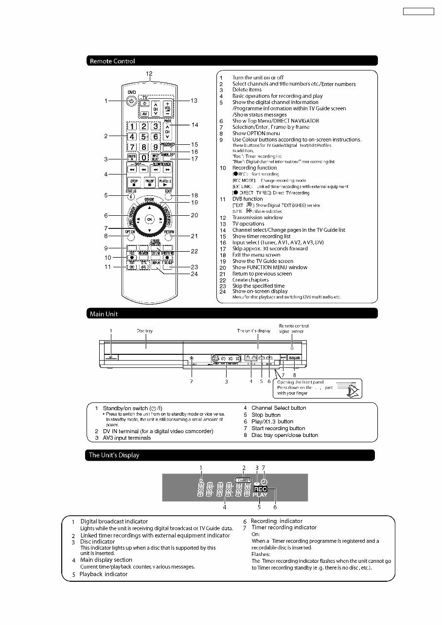
5 Location of Controls and Components
9
DMR-EZ27EB

6 Operation Instructions
6.1. Taking out the Disc from DVD-Drive Unit when the Disc cannot be
ejected by OPEN/CLOSE button
6.1.1. Forcible Disc Eject
6.1.1.1. When the power can be turned off.
1. Turn off the power and press [STOP] [CH UP] keys on the front panel simultaneously for 5 seconds.
6.1.1.2. When the power can not be turned off.
1. Press [POWER] key on the front panel for over 10 seconds to turn off the power forcibly, and press [STOP] [CH UP] keys on
the front panel simultaneously for 5 seconds.
10
DMR-EZ27EB
You're Reading a Preview
What's Included?
 Lifetime Access
Fast Download Speeds
Online & Offline Access
Access PDF Contents & Bookmarks
Full Search Facility
Print one or all pages of your manual
$35.99
Panasonic DMR-EZ27 EZ27EB Service Manual and Repair Guide
Viewed 75 Times Today

What's Included?
Lifetime Access
Fast Download Speeds
Online & Offline Access
Access PDF Contents & Bookmarks
Full Search Facility
Print one or all pages of your manual
$35.99

Secure transaction
What's Included?
Lifetime Access
Fast Download Speeds
Online & Offline Access
Access PDF Contents & Bookmarks
Full Search Facility
Print one or all pages of your manual
Description
This official service and repair manual is an invaluable resource for professional mechanics and DIY enthusiasts alike. It provides comprehensive information on safety and service precautions, specifications and operations, service modes, disassembly and assembly instructions, measurements and adjustments, block diagrams, schematic diagrams, printed circuit boards, exploded views, and a parts list catalog.
Rest assured, this manual is not a scanned-in or bootlegged copy. It is created in the highest resolution, ensuring excellent print quality for all pages. With instant access, there are no shipping fees or waiting on postal delivery, allowing you to commence repairs promptly.
- Language: English
- Format: .PDF
- Pages: 85


