

Denon AVR 1602 + 682 Service Manual & Repair Guide
What's Included?
Fast Download Speeds
Online & Offline Access
Access PDF Contents & Bookmarks
Full Search Facility
Print one or all pages of your manual
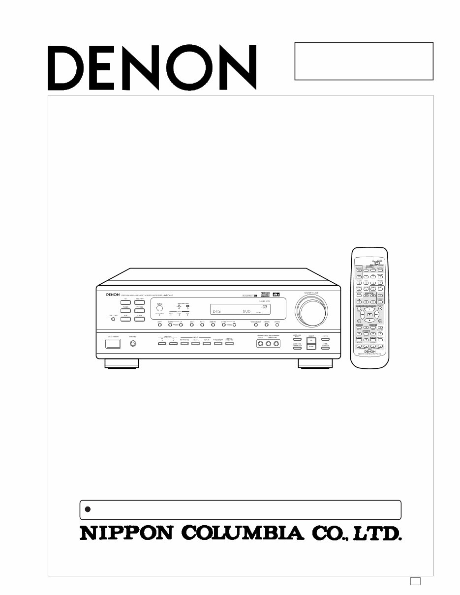
Hi-Fi Component
SERVICE MANUAL
MODEL AVR-1602/682
AV SURROUND RECEIVER
Some illustrations using in this service manual are slightly different from the actual set.
14-14, AKASAKA 4-CHOME, MINATO-KU, TOKYO 107-8011 JAPAN
Telephone: 03 (3584) 8111
X0116 1174 NC 0111
For U.S.A., Canada, Europe,
Asia, China, Hong Kong &
Taiwan R.O.C. model
2
AVR-1602/682
SPECIFICATIONS
SAFETY PRECAUTIONS
The following check should be performed for the continued protection of the customer and service technician.
LEAKAGE CURRENT CHECK
Before returning the unit to the customer, make sure you make either (1) a leakage current check or (2) a line to chassis
resistance check. If the leakage current exceeds 0.5 milliamps, or if the resistance from chassis to either side of the
power cord is less than 460 kohms, the unit is defective.
Audio Section
Power Amplifier
Rated output: Front: 70W+70W (8Ω/ohms, 20Hz~20kHz with 0.08% T.H.D )
100W+100W (6Ω/ohms, 1kHz with 0.7% T.H.D ) (U.S.A., Canada & Europe Models)
110W+110W (6Ω/ohms, EIAJ ) (Asia Model)
Center: 70W (8Ω/ohms, 20Hz~20kHz with 0.08% T.H.D )
100W (6Ω/ohms, 1kHz with 0.7% T.H.D ) (U.S.A., Canada & Europe Models)
110W (6Ω/ohms, EIAJ ) (Asia Model)
Surround: 70W+70W (8Ω/ohms, 20Hz~20kHz with 0.08% T.H.D )
100W+100W (6Ω/ohms, 1kHz with 0.7% T.H.D ) (U.S.A., Canada & Europe Models)
110W+110W (6Ω/ohms, EIAJ ) (Asia Model)
Output terminals: Front: A or B 6 to 16W/ohms
A+B 12 to 16W/ohms
Center/Surround: 6 to 16W/ohms
Analog
LINE input - PRE OUT
Input sensitivity/input impedance: 200mV/47kΩ/kohms
Frequency response: 10Hz~100kHz: +1, −3dB (TONE DEFEAT ON)
S/N ratio: 98dB (IHF-A weighted) (TONE DEFEAT ON)
Video Section
Standard video jacks
Input/output level and impedance: 1Vp-p,75Ω/ohms
Frequency response: 5Hz~10MHz +1, −3dB
S-video jacks (U.S.A., Canada & Asia Models)
Input/output level and impedance: Y(brightness)signal 1Vp-p, 75Ω/ohms
C(color)signal 0.286Vp-p, 75Ω/ohms
Frequency response: 5Hz~10MHz: +1, −3dB
Tuner section
Receiving range: [FM] (note: µV at 75Ω/ohms, 0dBf =1×10
-15
W) [AM]
U.S.A., Canada Models: 87.50MHz~107.90MHz 520kHz~1710kHz
Europe & Asia (for China) Models: 87.50MHz~108.00MHz 522kHz~1611kHz
Asia (for Multiple voltage) Models: 87.50MHz~107.90MHz (0.2MHz steps) 520kHz~1710kHz (10kHz steps)
87.50MHz~108.00MHz (0.05MHz steps) 522kHz~1611kHz (9kHz steps)
Usable sensitivity: 1.0µV (11.2dBf) 18µV
50 dB quieting sensitivity: MONO 1.6µV (15.3dBf)
STEREO 23µV (38.5dBf)
S/N ratio: MONO 80dB (IHF-A weighted)
STEREO 75dB (IHF-A weighted)
Total harmonic distortion: MONO 0.15% (1kHz)
STEREO 0.3% (1kHz)
General
Power supply:
U.S.A., Canada Models AC120V,60Hz
Europe Model AC230V,50Hz
Asia(for Multiple voltage)Model AC115/230V,50/60Hz
Asia(for China)Model AC220V,50Hz
Power consumption: 3.7A (USA & Canada model), 200W (Europe & Asia model)
Maximum external dimensions: 434 (W) × 147 (H) × 417 (D) mm (17-3/32″ × 5-25/32″ × 16-7/16″)
Mass: 9.8kg (20 lbs 9.7 oz)
Remote control unit (RC-896)
Batteries: R6P/AA Type (two batteries)
External dimensions: 54 (W) × 172.5 (H) × 29 (D) mm (2-1/8″ × 6-51/64″ × 1-9/64″)
Mass: 120g (Approx. 4.2 oz) (including batteries)
* For purposes of improvement, specifications and design are subject to change without notice.
AVR-1602/682
3
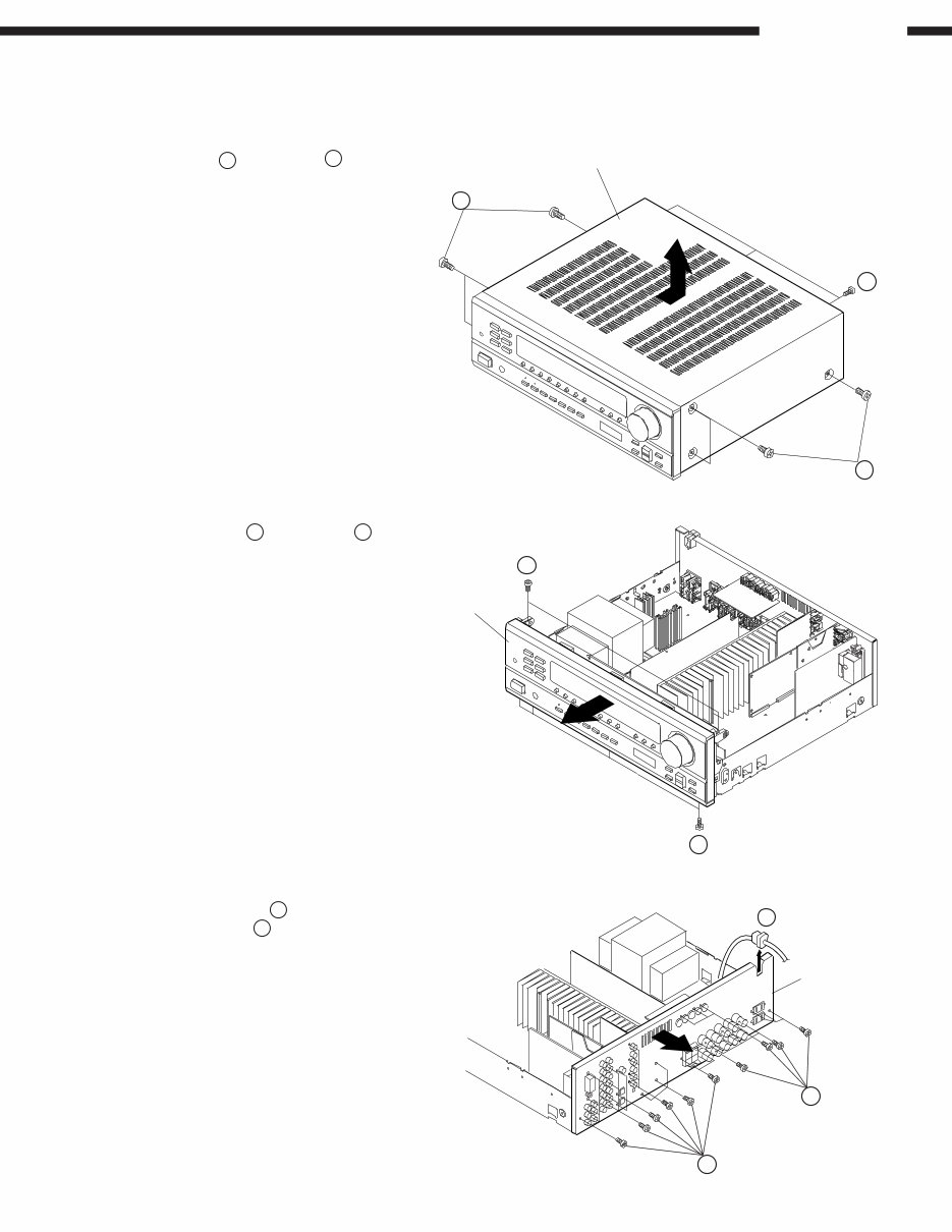
DISASSEMBLY
(Follow the procedure below in reverse order when reassembling)
Top Cover
Remove 6 screws 1 and 3 screws 2 , detach the Top Cover
in the arrow direction.
Top Cover
Front Panel
1. Remove 4 screws 3 and 2 screws 4 .
2. Detach the Front Panel in the arrow direction.
Front Panel
1
1
2
4
3
Rear Panel
1. Remove cord bushing 5 from the Rear Panel.
2. Remove 31 screws 6 .
3. Detach the Rear Panel in the arrow direction.
6
6
Rear Panel
5
8 7 6 5 4 3 2 1
A
B
C
D
E
AVR-1602/682
4
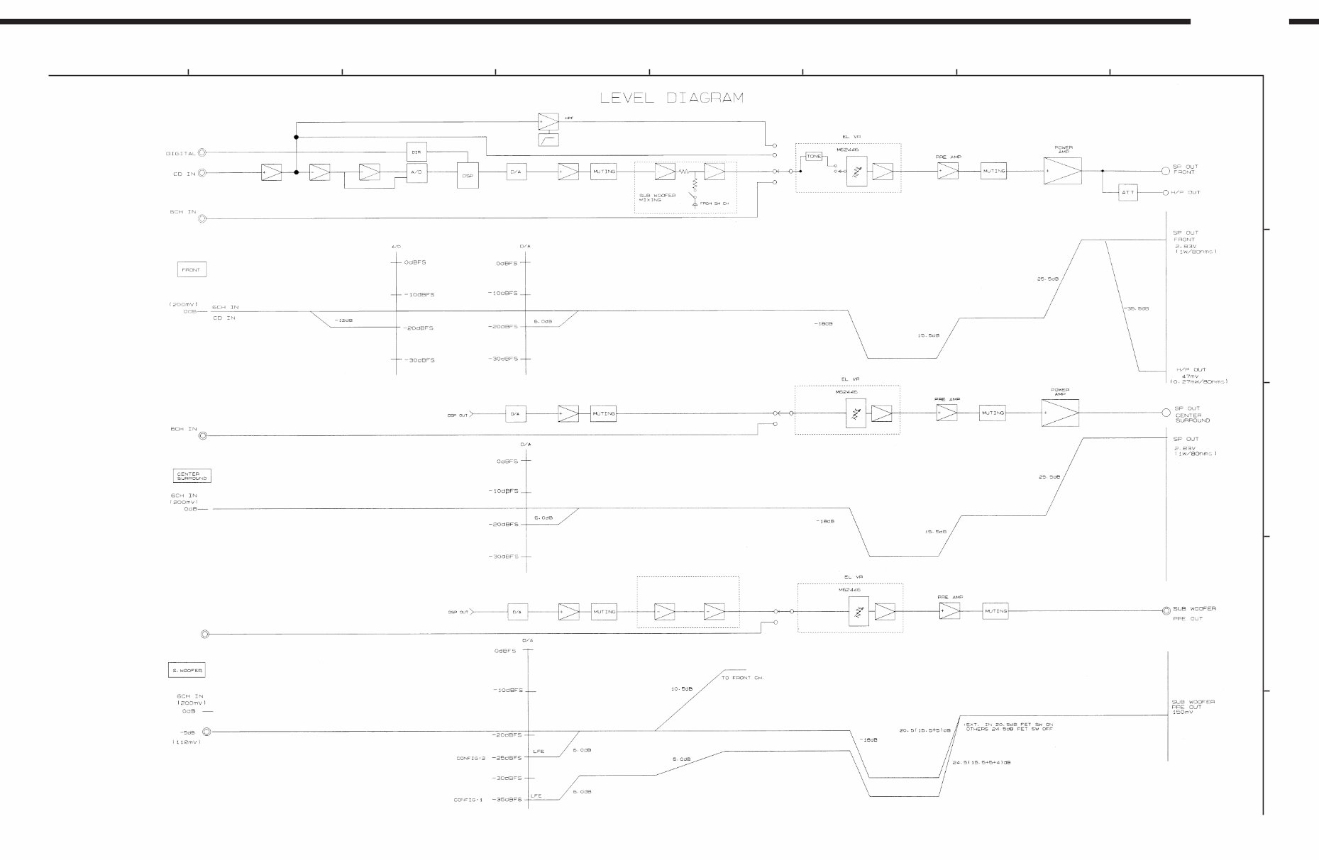
LEVEL DIAGRAM
8 7 6 5 4 3 2 1
A
B
C
D
E
AVR-1602/682
5
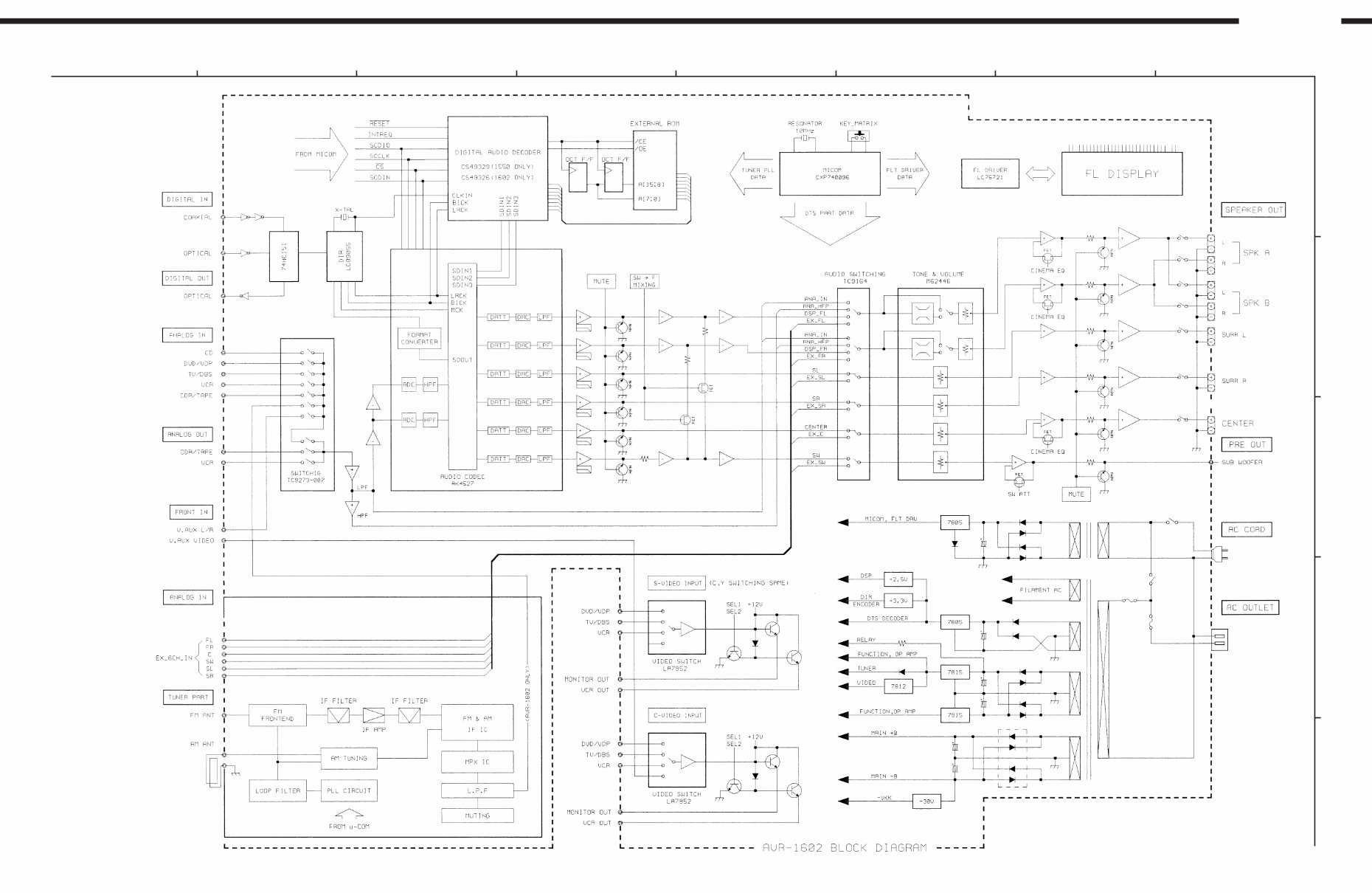
BLOCK DIAGRAM
AVR-1602/682
6
FM ALIGNMENT
Input Output Adjustment
Step
Alignment
Item
Tuning
Frequency
Setting
Type Frequency
Input
Level
Modulation Coupling Type Connect to Points Adjust to
1
Center
Adjustment
98.1MHz
(98.0MHz)
FM SSG 98.1MHz 60dB
Mono
1kHz 100%
Antenna
Terminal
Digital
Voltmeter
R471 T402 50mV
2 Distortion
98.1MHz
(98.0MHz)
FM SSG 98.1MHz 60dB
Mono
1kHz 100%
Antenna
Terminal
Distortion
Meter
Output
Terminal (L)
T403
Minimum
Distortion
3 Repeat Steps 1 and 2
4 Signal Level
98.1MHz
(98.0MHz)
FM SSG 98.1MHz 20dB OFF
Antenna
Terminal
Light “TUNED” on
FL Display
VR402
ADJUSTMENT
Tuner Section
CONNECTION DIAGRAM OF MEASURING INSTRUMENTS
FM
STEREO
MODULATOR
FM SSG
Digital
Voltmeter
75ohm
T402 T403
IC402
VR402
TUNER B'D
R471
20
+14
−10 dB
AM
T402 T403
IC402
TUNER B’D
R471
VR401
AM ALIGNMENT
Output Adjustment
Step
Alignment
Item
Frequency Input
Type Connect to Points Adjust to
Remarks
1 Signal Level
999 (1000)
kHz
AM SSG VR401
Light “TUNED” on
FL Display
SSG OUTPUT
74dB (EMF)
AVR-1602/682
7
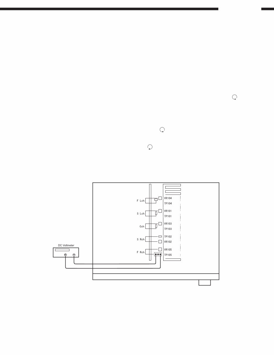
Audio Section
Idling Current
Required measurement equipment : DC Voltmeter
Preparation
(1) Avoid direct blow from an air conditioner or an electric fan, and adjust the unit at normal room tempereture
15 °C ~ 30 °C (59 °F ~ 86 °F).
(2) Presetting
● POWER (Power sourse switch) → OFF
● SPEAKER (Speaker terminal) → No load (Do not connect speaker, dummy resistor, etc.)
Adjustment
(1) Remove top cover and set VR101, VR102, VR103, VR104, VR105 on Amp. Unit at full counterclockwise ( )
position.
(2) Connect DC Voltmeter to test points (FRONT-Lch: TP104, FRONT-Rch: TP105, CENTER ch: TP103,
SURROUND-Lch: TP101, SURROUND-Rch: TP102).
(3) Connect power cord to AC Line, and turn power switch "ON".
(4) Presetting. MASTER VOLUME : "---" counterclockwise ( min.)
MODE : 5CH STEREO
FUNCTION : CD
(5) Within 2 minutes after the power on, turn VR101 clockwise ( ) to adjust the TEST POINT voltage to 1.5 mV ±0.5 mV
DC.
(6) After 10 minutes from the preset above, turn VR101 to set the voltage to 2.5 mV ±0.5 mV DC.
(7) Adjust the Variable Resistors of other channels in the same way.
AVR-1602/682
8
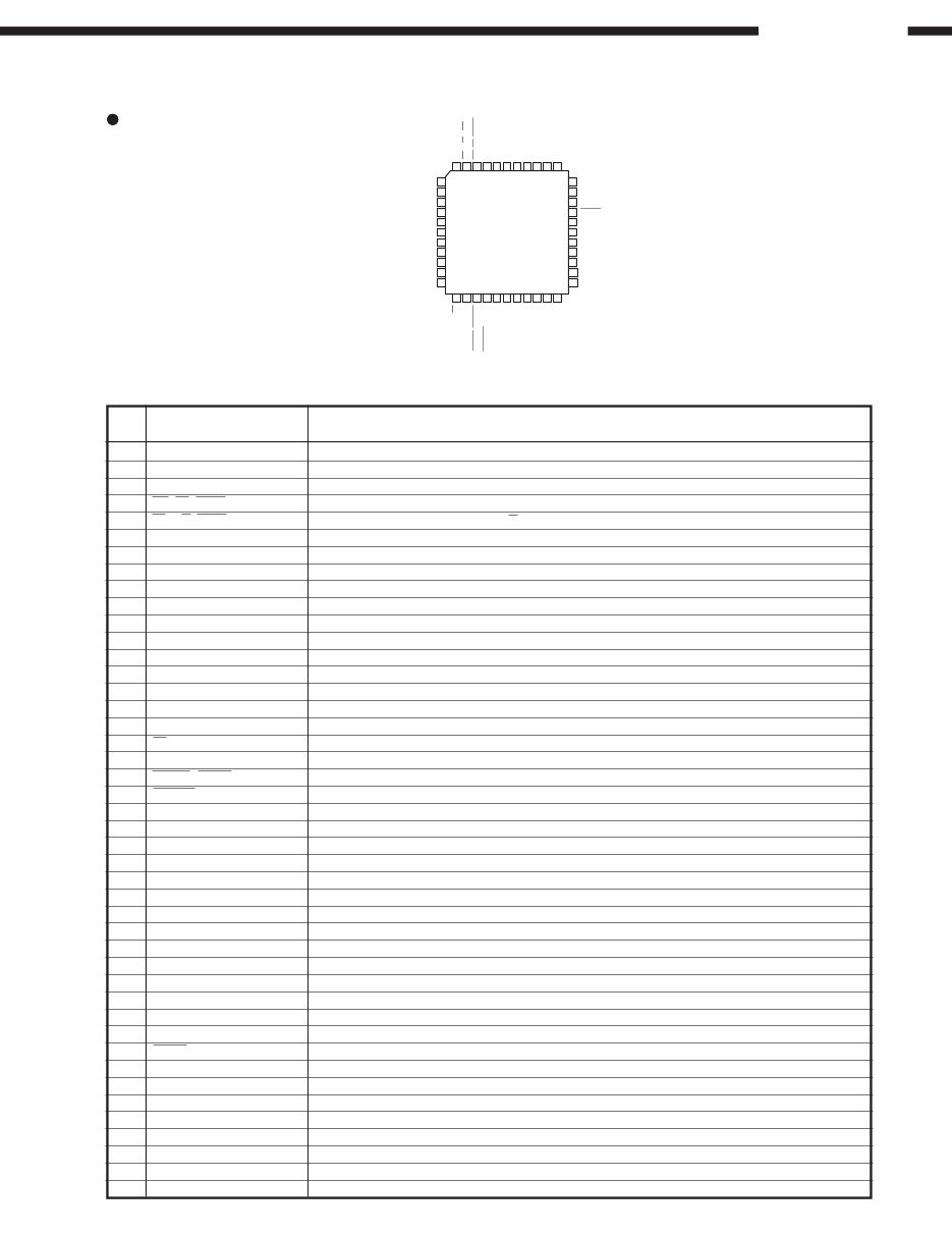
1 2 3 4 5 6
7
8
9
10
11
33
32
31
30
29
28 27 26 25 24 23
34
35
36
37
38
39
40 41 42 43 44
17
16
15
14
13
12
18 19 20 21 22
A1,SCDIN
RD,R/W,EMOE,GPIO11
WR,DS,EMWR,GPIO10
AUDATA3,XMT958
DGND1
VD1
MCLK
SCLK
LRCLK
AUDATA0
AUDATA1
AUDATA2
DC
DD
RESET
AGND
VA
FILT1
FILT2
CLKSEL
CLKIN
CMPREQ,LRCLKN2
CS
SCDIO,SCDOUT,PSEL,GPIO9
ABOOT,INTREQ
EXTMEM,GPIO8
SDATAN1
VD3
DGND3
SCLKN1,STCCLK2
LRCLKN1
CMPDAT,SDATAN2,RCV958
CMPCLK,SCLKN2
A0,SCCLK
DATA7,EMAD7,GPIO7
DATA6,EMAD6,GPIO6
DATA5,EMAD5,GPIO5
DATA4,EMAD4,GPIO4
VD2
DGND2
DATA3,EMAD3,GPIO3
DATA2,EMAD2,GPIO2
DATA1,EMAD1,GPIO1
DATA0,EMAD0,GPIO0
SEMICONDUCTORS
IC’s
CS49326-CL
(IC812)
CS49326-CL Terminal Function
1 VD1 Digital positive supply
2 DGND1 Digital supply ground
3 AUDATA3, XMT958 SPDIF transmitter output, Digital audio output 3
4 WR, DS, EMWR, GPIO10 Host write strobe or host data strobe or external memory write enable or general purpose input & output number 10
5 RD, R/W, EMOE, GPIO11 Host parallel output enable or host parallel R/W or external memory output enable or general purpose input & output number11
6 A1, SCDIN Host address bit one or SPI serial control data input
7 A0, SCCLK Host parallel address bit zero or serial control port clock
8 DATA7, EMAD7, GPIO7
9 DATA6, EMAD6, GPIO6
10 DATA5, EMAD5, GPIO5
11 DATA4, EMAD4, GPIO4
12 VD2 Digital positive supply
13 DGND2 Digital supply ground
14 DATA3, EMAD3, GPIO3
15 DATA2, EMAD2, GPIO2
16 DATA1, EMAD1, GPIO1
17 DATA0, EMAD0, GPIO0
18 CS Host parallel chip select, host serial SPI chip select
19 SCDIO, SCDOUT, PSEL, GPIO9 Serial control port data input and output, parallel port type select
20 INTREQ, ABOOT Control port interrupt request, automatic boot enable
21 EXTMEM, GPIO8 External memory chip select or general purpose input & output number 8
22 SDATAN1 PCM audio data input number one
23 VD3 Digital positive supply
24 DGND3 Digital supply ground
25 SCLKN1, STCCLK2 PCM audio input bit clock
26 LRCLKN1 PCM audio input sample rate clock
27 CMPDAT, SDATAN2, RCV958 PCM audio data input number two
28 CMPCLK, SCLKN2 PCM audio input bit clock
29 CMPREQ, LRCLKN2 PCM audio input sample rate clock
30 CLKIN Master clock input
31 CLKSEL DSP clock select
32 FILT2 Phase locked loop filter
33 FILT1 Phase locked loop filter
34 VA Analog positive supply
35 AGND Analog supply ground
36 RESET Master reset input
37 DD Reserved
38 DC Reserved
39 AUDATA2 Digital audio output 2
40 AUDATA1 Digital audio output 1
41 AUDATA0 Digital audio output 0
42 LRCLK Audio output sample rate clock
43 SCLK Audio output bit clock
44 MCLK Audio master clock
Pin
No.
Pin Name Function
AVR-1602/682
9
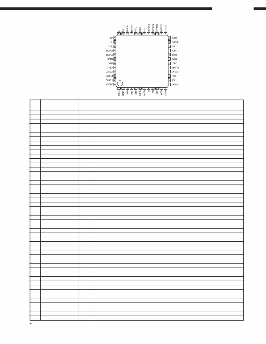
LC89055W (IC810)
LC89055W Terminal Function
1 DISEL I Data input terminal (select input pin of DIN0, DIN1)
2 DOUT O Input bi-phase data through output terminal
3 DIN0 I Amp built-in coaxial/optical input correspond data input terminal
4 DIN1 I Amp built-in coaxial/optical input correspond data input terminal
5 DIN2 I Optical input correspond data input terminal
6 DGND Digital GND
7 DVDD Digital power supply
8 R I VCO gain control input terminal
9 VIN I VCO free-run frequency setting input terminal
10 LPF O PLL loop filter setting terminal
11 AVDD Analog power supply
12 AGND Analog GND
13 CKOUT O Clock output terminal (256fs, 384fs, 512fs, X’tal osc., VCO free-run osc.)
14 BCK O 64fs clock output terminal
15 LRCK O fs clock output terminal (L: Rch, H: Lch, I
2
S: Reverse)
16 DATAO O Data output terminal
17 XSTATE O Input data detecting result output terminal
18 DGND Digital GND
19 DVDD Digital power supply
20 XMCK O X’tal osc. clock output terminal (24.576MHz or 12.288MHz)
21 XOUT O X’tal osc. connection output terminal
22 XIN I X’tal osc. connection input terminal, external signal input possible (24.576MHz or 12.288MHz)
23 EMPHA O Emphasis information output terminal of channel status
24 AUDIO O Bit1 output terminal of channel status
25 CSFLAG O Top 40bit revise flag output terminal of channel status
26 F0/P0/C0 O Input fs cal. sig. out/data type out/input word inf. output terminal
27 F1/P1/C1 O Input fs cal. sig. out/data type out/input word inf. output terminal
28 F2/P2/C2 O Input fs cal. sig. out/data type out/input word inf. output terminal
29 VF/P3/C3 O Validity flag out/data type out/input word inf. output terminal
30 DVDD Digital power supply
31 DGND Digital GND
32 AUTO O Non PCM burst data transfer detect sig. output terminal
33 BPSYNC O Non PCM burst data preamble Pa, Pb, Pc, Pd sync sig. output terminal
34 ERROR O PLL lock error, data error flag output terminal
35 DO O CPU/IFD read data output terminal
36 DI I CPU I/F write data input terminal
37 CE I CPU I/F chip enable input terminal
38 CL I CPU I/F chip enable input terminal
39 XSEL I Frequency select input pin of XIN X’tal osc. (24.576MHz or 12.288MHz)
40 MODE0 I Mode setting input terminal
41 MODE1 I Mode setting input terminal
42 DGND Digital GND
43 DVDD Digital power supply
44 DOSEL0 I Data output format select input terminal
45 DOSEL1 I Data output format select input terminal
46 CKSEL0 I Output clock select input terminal
47 CKSEL1 I Output clock select input terminal
48 XMODE I Reset input terminal
Pin
No.
Pin Name Function I/O
For latch-up countermeasure, set digital (DVDD) and analog (AVDD) power on/off in the same timing.
AVR-1602/682
10
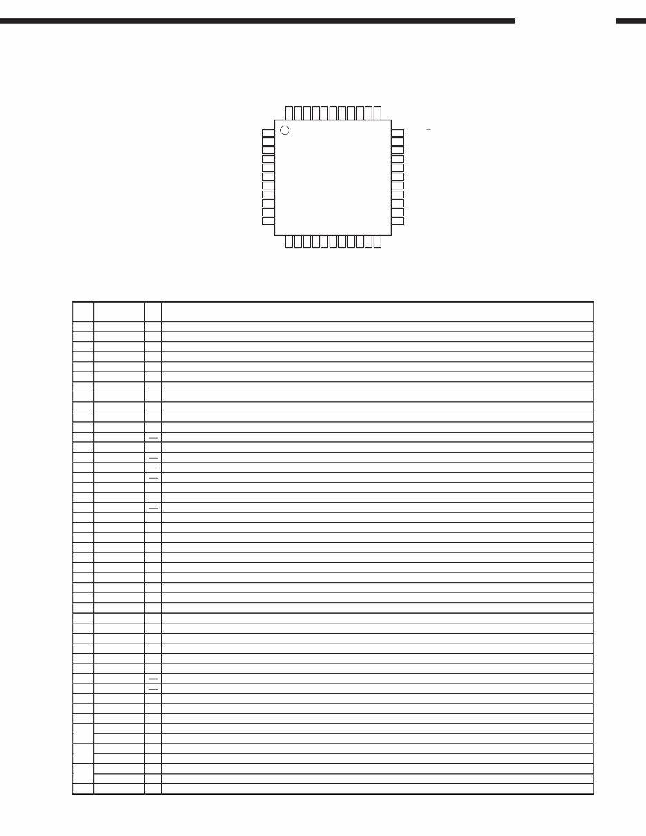
AK4527BVQ (IC813)
AK4527BVQ Terminal Function
1
2
3
4
5
6
7
8
9
10
11
12 13 14 15 16 17 18 19 20 21 22
33
32
31
30
29
28
27
26
25
24
23
44 43 42 41 40 39 38 37 36 35 34
SDOS
I2C
SMUTE
BICK
LRCK
SDTI1
DAUX
DFS
DZ F2/OVF
RIN+
RIN–
ROUT1
L0OP1
L0OP0/SDA/CDTI
DIF1/SCL/CCLK
DIF0/CSN
P/S
MCLK
DZF1
AVSS
AVDD
VREFH
VCOM
NC
TVDD
PDN
TST
CAD1
LIN+
LIN–
LOUT1
ROUT2
LOUT2
ROUT3
LOUT3
SDTI2
SDTI3
SDTO
DZ FE
DVDD
DVSS
NC
ADIF
CAD0
Top View
AK4527BVQ
Pin
No.
Pin Name I/O Function
1 SDOS I SDTO source select pin, L: Internal ADC output, H: DAUX input
2 I2C I Serial control mode select pin, L: 3-core serial, H: I
2
C bus
3 SMUTE I Soft mute pin, H: Soft mute start, L: Release
4 BICK I Audio serial data clock pin
5 LRCK I Input channel clock pin
6 SDTI1 I DAC1 audio serial data input pin
7 SDTI2 I DAC2 audio serial data input pin
8 SDTI3 I DAC3 audio serial data input pin
9 SDTO O Audio serial data output pin
10 DAUX I Auxiliary audio serial data input pin
11 DFS I Double speed sampling mode pin, L: Normal, H: Double
12 NC No Connect, No internal bonding
13 DZFE I Zero input detect enable pin
14 TVDD Power pin for output buffer, 2.7V~5.5V
15 DVDD Digital power pin, 4.5V~5.5V
16 DVss Digital GND pin, 0V
17 PDN I Power down & reset pin, L: Powered-down and register initialized, Reset with PDN when switching P/S or CAD0-1
18 TST I Test pin, connected to DVSS
19 NC No Connect, No internal bonding
20 ADIF I Analog Input Format Select pin
21 CAD1 I Chip address-1 pin
22 CAD0 I Chip address-0 pin
23 LOUT3 O DAC3L channel analog out pin
24 ROUT3 O DAC3R channel analog out pin
25 LOUT2 O DAC2L channel analog out pin
26 ROUT2 O DAC2R channel analog out pin
27 LOUT1 O DAC1L channel analog out pin
28 ROUT1 O DAC1R channel analog out pin
29 LIN- I L-ch analog inverted input pin
30 LIN+ I L-ch analog non-inverted input pin
31 RIN- I R-ch analog inverted input pin
32 RIN+ I R-ch analog non-inverted input pin
33 DZF2/OVF O 0 input detect 2 pin/Analog input overflow detect pin
34 VCOM O Common V-out pin, AVDD/2, connect large capacitor to avoid noise
35 VREFH I Ref. V input pin, AVDD
36 AVDD Analog GND pin, 4.5V~5.5V
37 AVss Analog GND pin, 0V
38 DZF1 O 0 input detect pin, H: Input data of G1 is 8192 times “0” in a raw or RSTN bit “0”
39 MCLK I Master clock input pin
40 P/S I Parallel/Serial select pin, L: Serial control
DIF0 I Audio data I/F format 0 pin (parallel control)
41
CSN I Chip select pin (3-wire serial control), connect to DVDD when I
2
C bus control
DIFI I Audio data I/F format 1 pin (parallel control)
42
SCL/CCLK I Control data clock pin (serial control), I
2
C=”L”: CCLK (3-wire serial), I
2
C=”H”: SCL (I
2
C bus)
LOOP0 I Loop back mode 0 pin (parallel control), effects digital loop back ADC to all DAC
43
SDA/CDTI I/O Control data input pin (serial control), I
2
C=”L”: CCTI (3-wire serial), I
2
C =”H” SDA (I
2
C bus)
44 LOOP1 I Loop back mode 1 pin, from SDT1 to all DAC
You're Reading a Preview
What's Included?
Fast Download Speeds
Online & Offline Access
Access PDF Contents & Bookmarks
Full Search Facility
Print one or all pages of your manual
$31.99
Viewed 91 Times Today


Secure transaction
What's Included?
Fast Download Speeds
Online & Offline Access
Access PDF Contents & Bookmarks
Full Search Facility
Print one or all pages of your manual
$31.99
This Denon AVR 1602 + 682 Audio/Video Surround Receiver service and repair manual is an essential resource for both professional mechanics and DIY enthusiasts. It contains comprehensive technical information required for servicing and repairing the receiver.
- The manual is fully illustrated with schematic diagrams, block diagrams, printed circuit boards, terminal descriptions, exploded views, and a complete parts list catalog.
- It is the official service manual in high resolution format, providing in-depth insights into the receiver's functionality.
- Upon payment, you will gain instant access to the manual, enabling you to commence repairs promptly.
Specifications:
- Language: English
- Format: PDF
- Page: 48


