

1 2 3 4 5 6 7 8 9 10 11
A
B
C
D
E
F
G
H
<P.1>
CLP-130
CLP-130 CLP-130
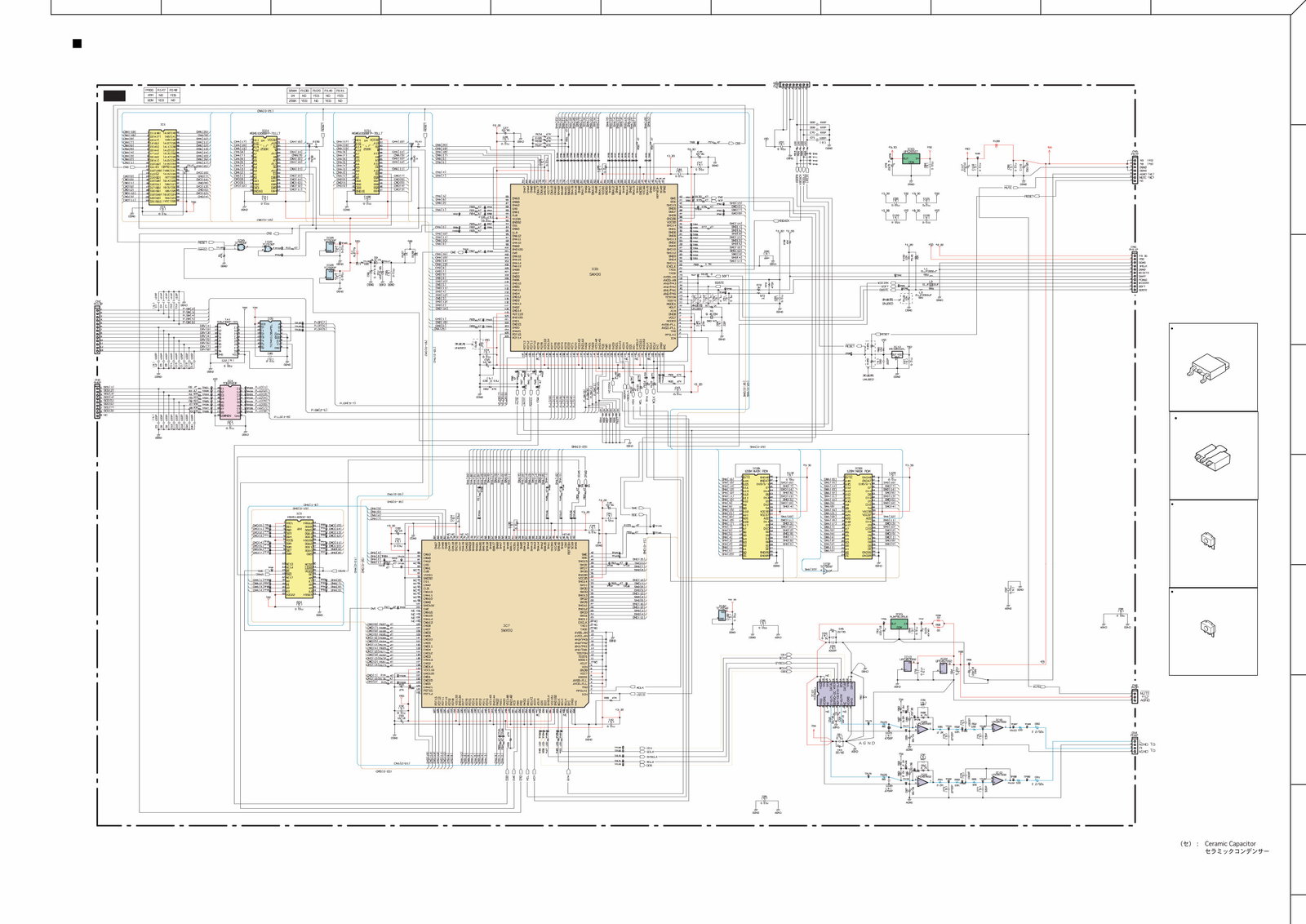
CLP-130 CIRCUIT DIAGRAM 1/3 (DM)
DM
NAND
OR
DEMULTIPLEXER
DRIVER ARRAY
SRAM SRAM
PROGRAM ROM
SWX00B
SWX00B
EFFECT DRAM
INVERTER
D/A CONVERTER
OP AMP
REGULATOR +5V
WAVE ROM 1 WAVE ROM 2
SYSTEM RESET
REGULATOR +3.3V
28CC1-8822660
to PNL-CN101
to PNR-CN201
to PNL-CN102
to PNR-CN202
to DJK-CN9
to DJK-CN4
to AJK-CN502
to AJK-CN501
to GHDcl SW L-CN1
µPC2933T(XS516A00)
REGULATOR +3.3V
1: V in
2: GND
3: V out
1
2
3
DM:IC015
µPC78L05T (XS721A00)
REGULATOR +5V
1: INPUT
2: GND
3: OUTPUT
1
3
2
DM:IC023
M51951AML(XR063A00)
SYSTEM RESET
1: SUPPLY
VOLTAGE
2: GND
3: OUTPUT
1
2
3
DM:IC012
NJM J78L05UA(XJ598A00)
REGULATOR +5V
1: OUTPUT
2: COMMON
3: INPUT
1
2
3
DM:IC023
Note: See parts list for details of citcuit baord component parts.
1 2 3 4 5 6 7 8 9 10 11
A
B
C
D
E
F
G
H
<P.2>
CLP-130
CLP-130 CLP-130
AJK
L (L+R)
R
AUX IN
From MA60-CN4
to DJK-CN10
to DM-CN4
to MA60-CN6
to HP-CN1
to DM-CN8
to PNL-CN301
AUX IN
(LEVEL FIXED)
L
R
L (L+R)
R
AUX OUT
28CC1-8822670
OP AMP
OP AMP
DJK
to DM-CN6
to DM-CN5
to MA60-CN4
to PEDAL (DJK)
-CN11
IN
OUT
THRU
MIDI
TO HOST
28CC1-8822661 1
INVERTER LINE RECEIVER
INVERTER
to AJK-CN540
to DJK-CN10
DESTINATION
DESTINATION
DESTINATION
Non connect
Non connect
to AJK-CN520
to SPEAKERS
NONPOLARIZED NONPOLARIZED NONPOLARIZED POLARIZED
Not installed Installed Not installed Not installed
Not installed Not installed Not installed
Not installed Not installed Not installed
Installed Not installed Installed Installed
28CB1-8811315 0
REGULATOR
REGULATOR
REGULATOR
AC IN
28CC1-8811550 1
NET1
FU60
MA60
to AJK-CN530
to PL-CN1
NORMAL
OFF
ON
(HP,SW)
PHONES
HP
28CC1-8822665
PEDAL
28CC1-8812279
to PEDAL JACK
-JK6
C8 100P
C10 100P
C11 100P
to DJK-CN3
28CC1-8822661 1
PEDAL (DJK)
to HP-CN2
28CC1-8822669
PL
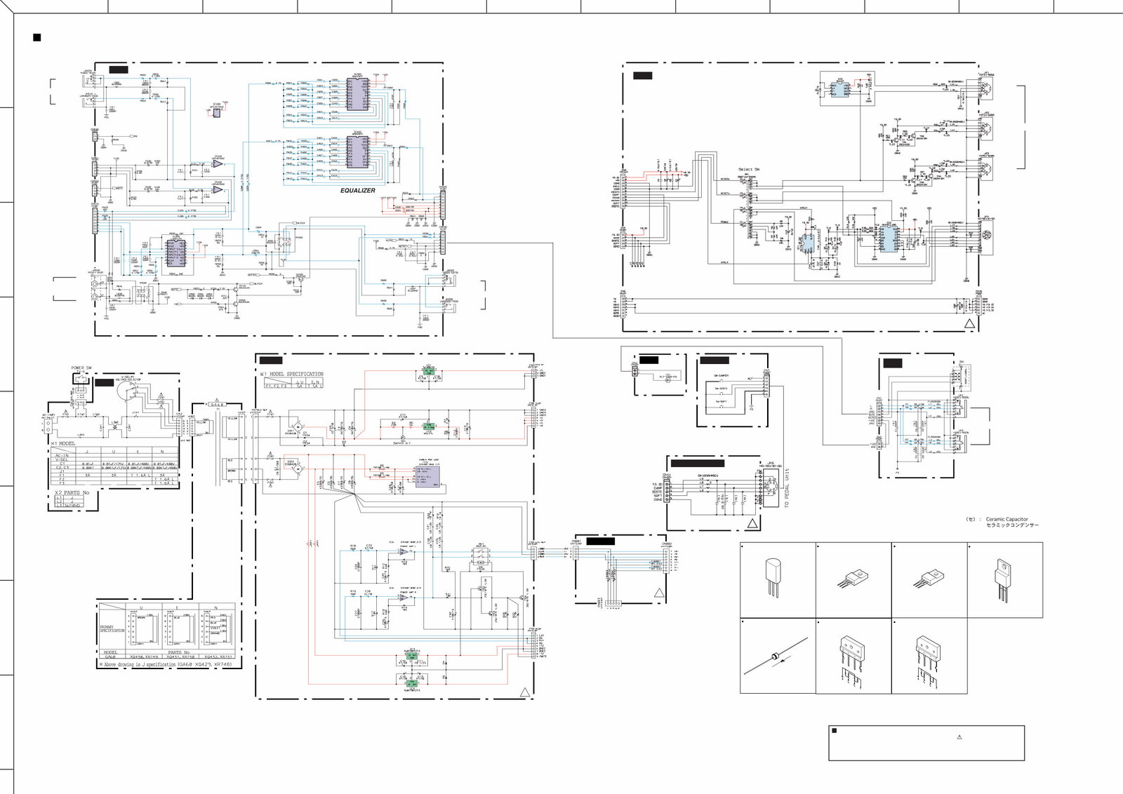
CLP-130 CIRCUIT DIAGRAM 2/3 (AJK, DJK, FU60, MA60, HP, PL, PEDAL JACK, PEDAL)
NJM78M12FA (XJ602A00)
REGULATOR +12V
1
2
3
1: OUTPUT
2: COMMON
3: INPUT
MA60:IC003
NJM79M12FA (XD343A00)
REGULATOR -12V
1
2
3
1: OUTPUT
2: INPUT
3: COMMON
MA60:IC004
SI-3051N (XQ437A00)
REGULATOR +5V
1: GND
2: OUTPUT
3: INPUT
3
2
1
MA60:IC001
Note: See parts list for details of citcuit baord component parts.
WARNING
Components having special characteristics are maked and
must be replaced with parts having specification equal to those originally installed.
D3SBA20-4103 (VQ111500)
DIODE STACK 4.0A
MA60:DB002
D5SBA20 (VK421800)
DIODE STACK 6.0A 200V
MA60:DB001
M5237L (XQ667A00)
REGULATOR +5V
1: INPUT
2: GND
3: VOLTAGE adj.
3
2
1
MA60:IC002
11ES4
(
VB481900
)
DIODE
1
2
1: ANODE
2: CATHODE
MA60:D1-D5
1 2 3 4 5 6 7 8 9 10 11
A
B
C
D
E
F
G
H
<P.3>
CLP-130
CLP-130 CLP-130
28CC1-8811214
to DM-CN3
2
28CC1-8811214
2
KSN2
GH-D_SW H
GH-D_SW L
D1
D2
D3
D4
Not install
Install
Not install
Not install
PNL
to AJK-CN510
to DM-CN1
to DM-CN2
28CC1-8822663
28CC1-8822664
PNR
to DM-CN1
to DM-CN2
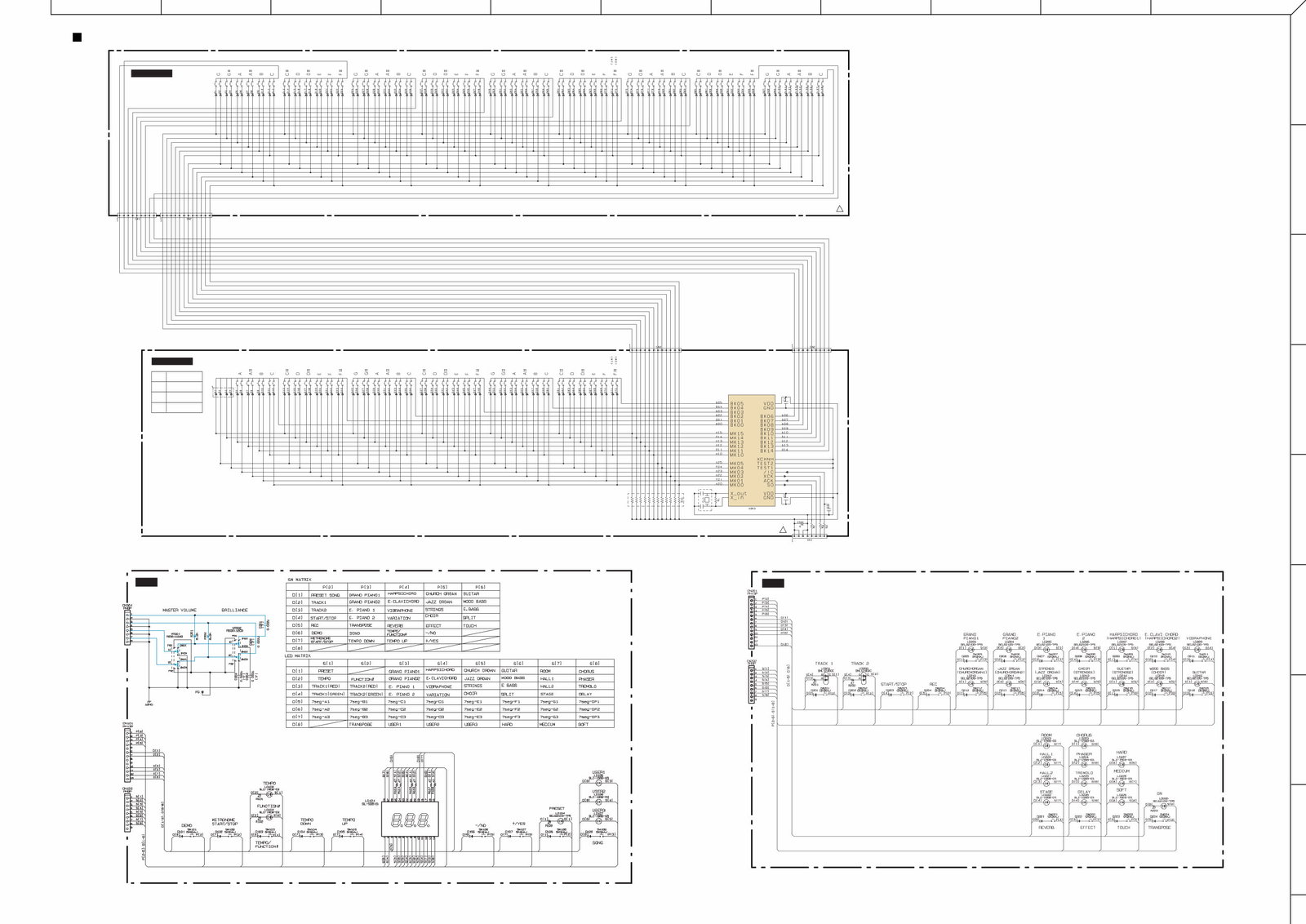
CLP-130 CIRCUIT DIAGRAM 3/3 (GH-D_SW H, GH-D_SW L, PNL, PNR)
Note: See parts list for details of citcuit baord component parts.
You're Reading a Preview
What's Included?
 Lifetime Access
Fast Download Speeds
Offline Viewing
Access Contents & Bookmarks
Full Search Facility
Print one or all pages of your manual
$30.99
Yamaha Clavinova CLP-130 Service Manual
Viewed 54 Times Today

What's Included?
Lifetime Access
Fast Download Speeds
Offline Viewing
Access Contents & Bookmarks
Full Search Facility
Print one or all pages of your manual
$30.99

Secure transaction
What's Included?
Lifetime Access
Fast Download Speeds
Offline Viewing
Access Contents & Bookmarks
Full Search Facility
Print one or all pages of your manual
Description
The Yamaha Clavinova CLP-130 Service Manual is a comprehensive resource covering a wide range of topics essential for servicing and repairing the Yamaha CLP-130 model. It includes detailed information on specifications, panel layout, circuit board layout, block diagram, disassembly procedure, LSI pin description, IC block diagram, circuit boards, inspection, MIDI implementation chart, overall circuit diagram, and a parts list.


