

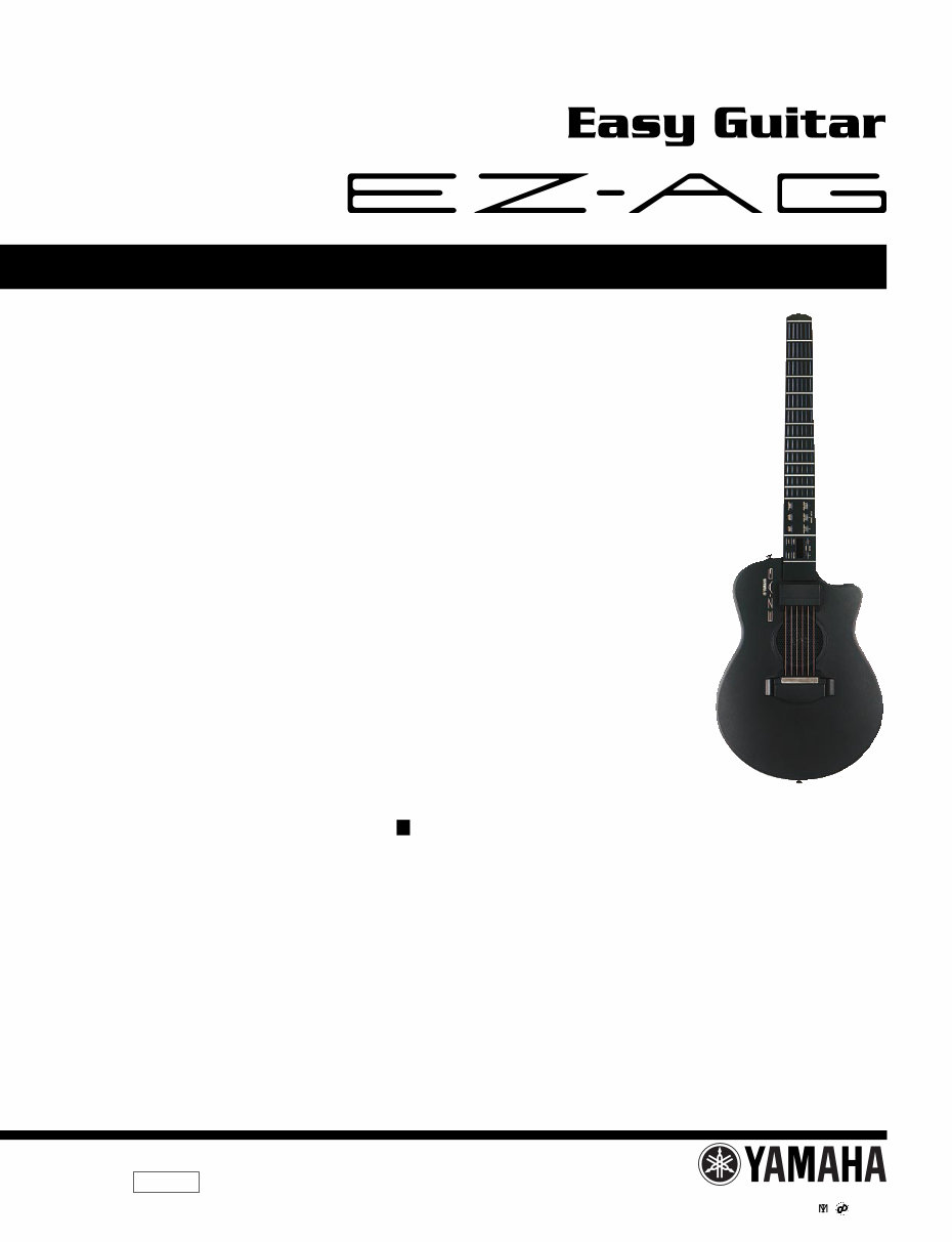
YAMAHA EZ-AG Service Manual
What's Included?
Fast Download Speeds
Online & Offline Access
Access PDF Contents & Bookmarks
Full Search Facility
Print one or all pages of your manual
SERVICE MANUAL
PK
011700
Copyright (c) Yamaha Corporation. All rights reserved. PDF-K167 ’03.11
HAMAMATSU, JAPAN
CONTENTS
SPECIFICATIONS ..................................................................... 3
PANEL LAYOUT ...................................................................... 4
CIRCUIT BOARD LAYOUT ...................................................... 5
BLOCK DIAGRAM .......................................................................... 6
DISASSEMBLY PROCEDURE ................................................. 7
LSI PIN DESCRIPTION ............................................................. 9
IC BLOCK DIAGRAM ............................................................. 11
CIRCUIT BOARDS .................................................................. 12
TEST PROGRAM ................................................................... 16
INSPECTION .......................................................................... 18
MIDI IMPLEMENTATION CHART ......................................... 19
PARTS LIST
OVERALL CIRCUIT DIAGRAM
EZ-AG
2
WARNING: CHEMICAL CONTENT NOTICE!
The solder used in the production of this product contains LEAD. In addition, other electrical/electronic and/or plastic (Where
applicable) components may also contain traces of chemicals found by the California Health and Welfare Agency (and possibly
other entities) to cause cancer and/or birth defects or other reproductive harm.
DO NOT PLACE SOLDER, ELECTRICAL/ELECTRONIC OR PLASTIC COMPONENTS IN YOUR MOUTH FOR ANY REASON WHAT
SO EVER!
Avoid prolonged, unprotected contact between solder and your skin! When soldering, do not inhale solder fumes or expose
eyes to solder/flux vapor!
If you come in contact with solder or components located inside the enclosure of this product, wash your hands before handling
food.
IMPORTANT NOTICE
This manual has been provided for the use of authorized Yamaha Retailers and their service personnel. It has been assumed
that basic service procedures inherent to the industry, and more specifically Yamaha Products, are already known and under-
stood by the users, and have therefore not been restated.
WARNING : Failure to follow appropriate service and safety procedures when servicing this product may result in per-
sonal injury, destruction of expensive components and failure of the product to perform as specified. For
these reasons, we advise all Yamaha product owners that all service required should be performed by an
authorized Yamaha Retailer or the appointed service representative.
IMPORTANT : This presentation or sale of this manual to any individual or firm does not constitute authorization certifi-
cation, recognition of any applicable technical capabilities, or establish a principal-agent relationship of
any form.
The data provided is belived to be accurate and applicable to the unit(s) indicated on the cover. The research engineering, and
service departments of Yamaha are continually striving to improve Yamaha products. Modifications are, therefore, inevitable
and changes in specification are subject to change without notice or obligation to retrofit. Should any discrepancy appear to
exist, please contact the distributor’s Service Division.
WARNING : Static discharges can destroy expensive components. Discharge any static electricity your body may have
accumulated by grounding yourself to the ground bus in the unit (heavy gauge black wires connect to
this bus.)
IMPORTANT : Turn the unit OFF during disassembly and parts replacement. Recheck all work before you apply power
to the unit.
WARNING
Components having special characteristics are marked and must be replaced with parts having specification equal to those
originally installed.
3
EZ-AG
SPECIFICATIONS
Strings
Frets
Displays
Sounds
Play Modes
Controls
Songs
Tempo Range
Volume Range
Balance Range
Capo Range
Tuning
Connectors
Maximum Output Power
PHONES/OUTPUT
Speaker
Power Supply
Power Consumption
Dimensions (w x d x h)
Weight
6
12
LED display, 6 x 6 fret LEDs
9 guitar, 8 bass, 3 others
STRUM (right hand), CHORD (left hand), BOTH (both hands)
[STANDBY/ON] switch, [STRUM] button, [CHORD] button, [BOTH] button,
[DEMO] button, [SOUND] button, [SONG] button, [TEMPO] button,
[VOLUME] button, [CAPO] button, [TUNING] button, VALUE [+]/[-] buttons
25 (additional songs can be loaded into internal memory from a computer)
32 - 280
0 - 127
0 - 127
0 - 6
28 tuning settings in addition to normal
DC IN 12V, PHONES/OUTPUT, MIDI IN and MIDI OUT
3.3 W (When using PA-3C AC adaptor)
1.4 W (batteries)
Output impedance: 77 Ω
10 cm
PA-3B or PA-3C AC Power Adaptor
Six 1.5 V LR6, ALKALINE “AA” SIZE
6.5 W (using the PA-3C)
863 x 307 x 81 mm (34" x 12" x 3-1/4")
1.9 kg (4 lbs. 3oz.) (w/o batteries)
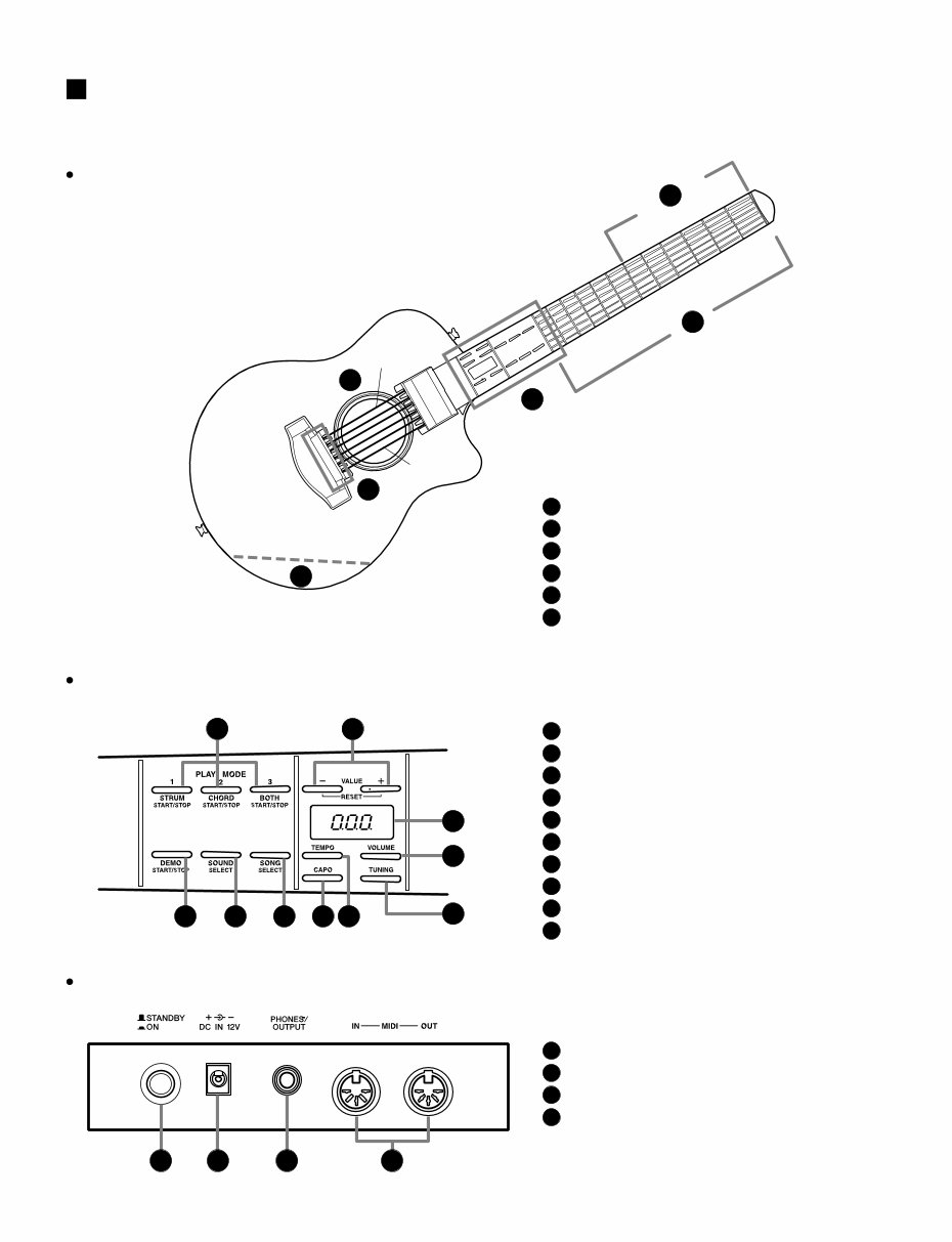
EZ-AG
4
1st
6th
2
3
1
5
6
7 16
17 18 19 20
8
9
10
11 12 13 14 15
4
1 LED
2 Frets
3 Control Section
7 VALUE [+]/[-] buttons
8 Display
9 [VOLUME] button
10 [TUNING] button
11 [TEMPO] button
12 [CAPO] button
13 [SONG] button
14 [SOUND] button
15 [DEMO] button
16 PLAY MODE
[1]/[STRUM], [2]/[CHORD], [3]/[BOTH] buttons
4 Strings
5 Bridge Plate
6 Connector & Power Switch Section
17 Power Switch ([STANDBY/ON])
18 DC IN 12V jack
20 MIDI IN/MIDI OUT connectors
19 PHONES/OUTPUT jack
Body
PANEL LAYOUT
Control Section
Connector & Power Switch Section
5
EZ-AG
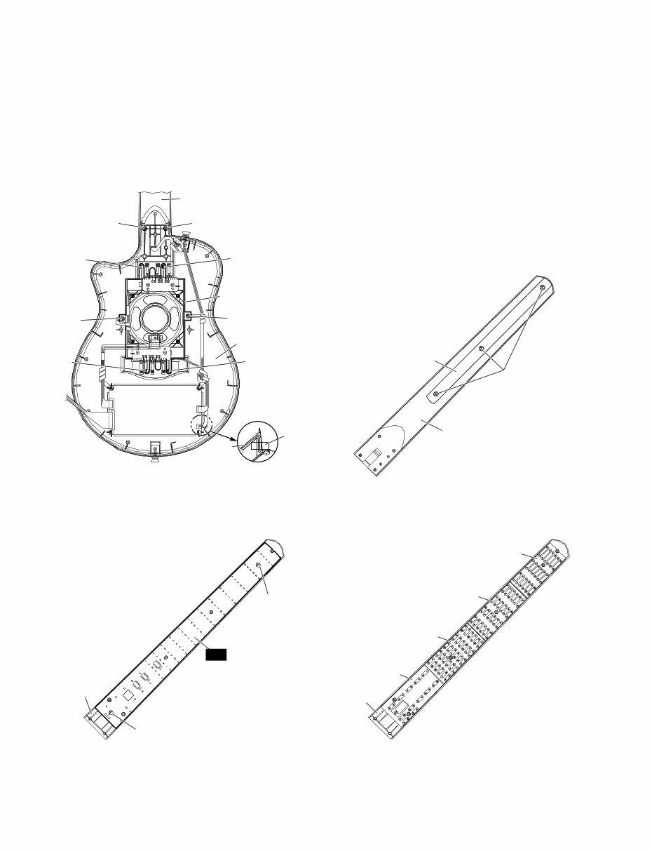
CIRCUIT BOARD LAYOUT
CN801 CN802
Neck assembly
Strings sensor unit
Bottom assembly
Top assembly
Battery cover assembly
<Bottom view>
<Top view>
<Bottom view>
<Bottom view>
SE1
PN
AM
DM
DM
SE
CN501 CN601
CN604 CN701
CN901 CN901 CN902 CN902
CN903
CN3 CN3
Adhesive
tape
MUTE
connector
assembly
• First lot
EZ-AG
6
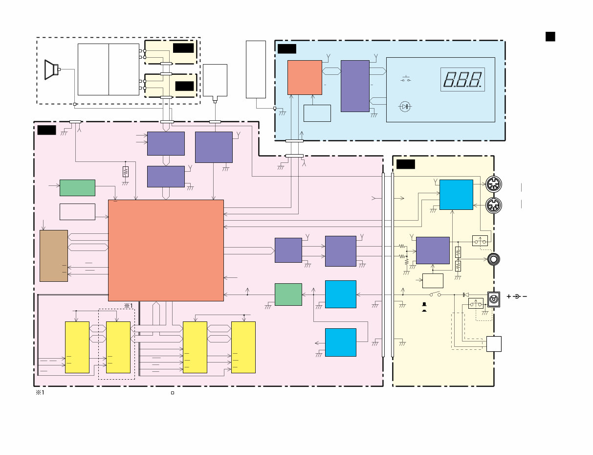
BLOCK DIAGRAM
SPEAKER
4 Ω
SENSOR
AMP 6ch
SE1
PN
AM
DM
SE
CN903 (4P)
S2
S1-S6
8X10
IC1 (64P)
TA1,3
(18P)
S4
S6
S1
S3
S5
CN902 (4P)
CN901 (7P)
SENSOR
UNIT
MUTE
PLATE
STRING
PIEZO
SENSOR
X3
PIEZO
SENSOR
X3
Earth
Plate
SUB
CPU
LED
Driver
CLOCK
8.00 MHz
DGND
15 36
S [0-11]
D [0-7]
L [0-15]
S [0-11]
D [0-7]
L [0-14]
X1
8,9
6,7
9,10
RXD
TXD
+5D
+3.3D
+5D
+5D +5D
+5D
JK702
(5P)
JK701
(5P)
to speaker
JK802
(8P)
JK801
(2P)
+5D
+5D
CN3 (5P)
SW MATRIX
7 Seg LED
X84
LD90
LED MATRIX
X36
D [0-7]
L [12-14]
CN601 (9P) CN604 (2P)
IC601-606 (8P)
CN602 (3P)
not used
+5D
+5D
8
4
-5D
RESET
3.6V
IC703 (5P)
CLOCK
8.4672MHz
MAIN
CPU
SWX00B
X102
IC201 (48P)
IC101 (168P)
ANALOG
SW
IC701 (16P)
SENSOR
AMP 1ch
(MUTE)
IC607 (14P)
FT [0-5] 1-3,5,12,13
5
4,14,15
8
16
6
+5D
7
14
+5D
+5D
5 4
1 17 14,15,16 152
DGND
IC AN3
TXD1
RXD1
TXD0
RXD0
AN0,AN1,
AN2
P-bus
MUT [0]
CN701 (5P)
CN501 (11P)
CN801 (11P)
SP
9,10
S-bus
47,48,51-59,62-71
23-34,37-40
41
74
WAVE
32M
MASK
+3.3D
1,37,38,47,48
SMA [0-20]
SMD [0-15]
OE
CE
27
24
SOE
SCSO
46,88,93
+3.3D
1,25,26,
37,38
12,14,27,
37,46,47
88,90,95,
101,131,132
106-118,
121-123
75,76,79-87,89
96-99,102-105,124
C-bus
PROGRAM
16M
P2ROM
IC302 (48P)
OE
CRD
CE
PROGRAM
16M
MASK
IC301 (48P)
OE
CE
2M
SRAM
IC303 (44P)
OE
39,40
11,13 37,47
CLB, CUB
CRD 41
17
6
28
11
26
CWE
CS2
CS3
WE
CE
4M
Flash
IC305 (48P)
OE
WE
CE
CS0, CS1
CS0
27 28
26 24
CMA [1-21] CMA [1-18]
CMD [0-15] CMD [0-15]
+3.3D
+3.3D
+5D
+5D
IC501 (8P)
4,7,18,35,49,61,
77,91,119,148
133,143,161
158,163,164
21 TX
MIDI-TX
MIDI-RX
RX 154
20
153
DO0,WCLK, QCLK
DAC
16Bit
IC102 (3P)
+3.3V
REG.
IC502 (8P)
LPF
&
AMP
IC503 (5P)
+5V
DC/DC
CNV.
MUTE
IC504 (8P)
-5V
DC/DC
CNV.
8
4
1
3
+5D
8
1
7
4
5,6,7
2,3
5,6
L
R
2
3
1
4
2
6
1
2,3
1
5
4
IC801 (10P)
TR703
IC701 (6P)
TR701,702
9
8
7
10,11
1
3
2
-5D
10,11
8
4
5
7
9
+12V
+5D
POWER
AMP
MIDI
I/F
MIDI
OUT
IN
PHONES/
OUTPUT
DC IN 12V
BATTERY
SUM3X6
(+9V)
STANDBY
ON
6
4
5
+12V
4
1
10
2
7
1
2
D801
SW801
Wire
-
+
CN802 (3P)
: IC301 or IC302 are mounted. : solder
28CA1-8826574
DGND
2,3
DGND
6
AGND
6
AGND
GND
7
EZ-AG
[140B]
[140B]
Top assembly
B
(Sensor wire)
Speaker
B (Sensor wire)
A
(Speaker terminals)
[110B]
[110B]
[110C]
[110C]
[110C]
[110C]
[110B]
[110B]
[130A]
<Bottom view>
SE
SE1
Adhesive
tape
MUTE
connector
assembly
• First lot
DM
[110A]
[110A]
[110A]
[120A]
[140A]
[140A]
Bottom assembly
<Bottom view>
[B120]
[B120]
[B120]
[B190]
Bottom assembly
AM
<Top view>
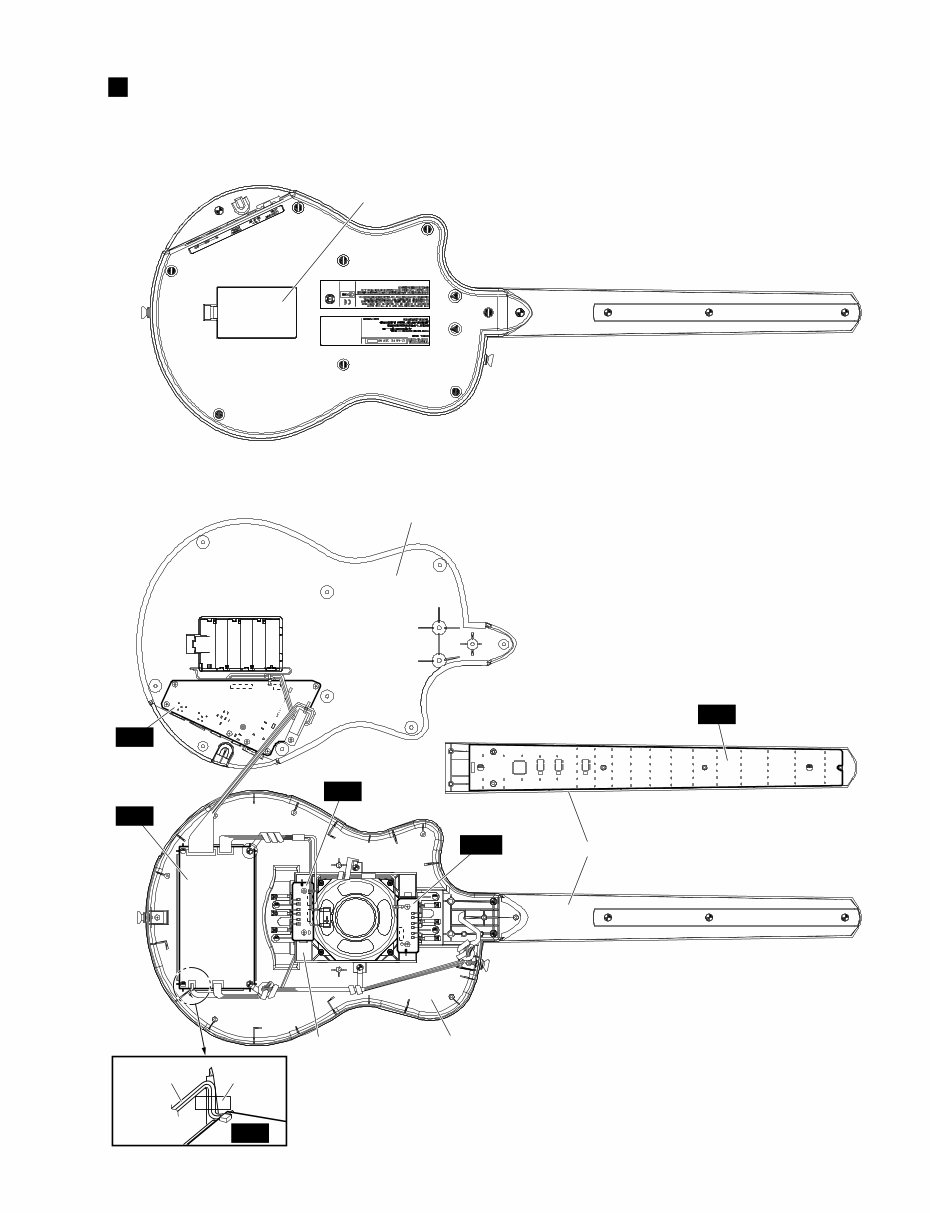
DISASSEMBLY PROCEDURE
1. Bottom Assembly
(Time required: About 2 minutes)
1-1 Remove the eight (8) screws marked [110A],the two
(2) screws marked [120A] and the two (2) screws
marked [140A]. The bottom assembly can then be
removed. (Fig. 1)
2. AM Circuit Board
(Time required: About 4 minutes)
2-1 Remove the bottom assembly. (See procedure 1.)
2-2 Remove the seven (7) screws marked [B120] and
the screw marked [B190]. The AM circuit board can
then be removed. (Fig. 2)
3. DM Circuit Board
(Time required: About 3 minutes)
3-1 Remove the bottom assembly. (See procedure 1.)
3-2 Remove the two (2) screws marked [130A] and the
two (2) screws marked [140B]. The DM circuit board
can then be removed. (Fig. 3)
4. SE (SE+SE1) Circuit Board, Speaker
4-1 Remove the bottom assembly. (See procedure 1.)
4-2 SE (SE+SE1) Circuit Board
(Time required: About 4 minutes):
4-2-1 Remove the four (4) screws marked [110B]. (Fig. 3)
4-2-2 Remove the solder from the two locations shown
as A (the speaker terminals) and then remove the
solder from the twelve locations shown as B (the
sensor wire). The SE (SE+SE1) circuit board can
then be removed. (Fig. 3)
4-3 Speaker (Time required: About 3 minutes):
4-3-1 Remove the four (4) screws marked [110C]. The
speaker can then be removed. (Fig. 3)
[110A]: Bind Head Tapping Screw-B 3.0X12 MFZN2Y (VE683000)
[120A]: Bind Head Tapping Screw-B 4.0X35 MFZN2Y (WB535600)
[140A]: Bind Head Tapping Screw-B 3.0X12 MFZN2BL (VQ074600)
(Fig. 1)
[B120]: Bind Head Tapping Screw-B 3.0X8 MFZN2Y (EP600250)
[B190]: Bind Head Tapping Screw-B 3.0X12 MFZN2BL (VQ074600)
(Fig. 2)
[110]: Bind Head Tapping Screw-B 3.0X8 MFZN2Y (EP600250)
[130A]: Bind Head Tapping Screw-B 3.0X8 MFZN2Y (EP600250)
[140B]: Bind Head Tapping Screw-B 3.0X12 MFZN2BL (VQ074600)
(Fig. 3)
Caution: Be sure to attach the removed filament tape just as it was before removal.
EZ-AG
8
Adhesive
tape
MUTE
connector
assembly
• First lot
Top assembly
Strings sensor unit
Neck assembly
[140C]
[130B] [130B]
[140C]
[130B]
[120B] [120B]
[130B]
<Bottom view>
Fingerboard
Key top rubber A
Key top rubber B
Key top rubber C
Key top rubber D
[N70]
Fingerboard
[N70]
<Bottom view> <Bottom view>
PN
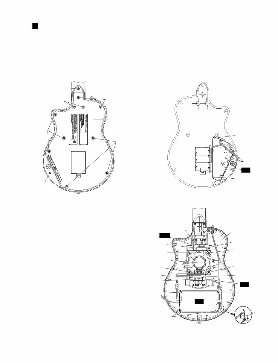
5. Strings Sensor Unit
(Time required: About 3 minutes)
5-1 Remove the bottom assembly. (See procedure 1.)
5-2 Remove the four (4) screws marked [130B] and the
two (2) screws marked [140C]. The strings sensor
unit can then be removed. (Fig. 4)
6. PN Circuit Board, Key Top Rubber
(Time required: About 4 minutes)
6-1 Remove the bottom assembly. (See procedure 1.)
6-2 Remove the three (3) screws marked [N100]. The
earth plate can then be removed. (Fig. 5)
6-3 Remove the two (2) screws marked [120B]. The
neck assembly can then be removed. (Fig. 4)
(Come off the wire from the connector of the neck
assembly side.)
6-4 Remove the two (2) screws marked [N70] from the
fingerboard. The PN circuit board and the key top
rubber can then be removed. (Fig. 6, 7)
[120B]: Bind Head Tapping Screw-B 4.0X35 MFZN2Y (WB535600)
[130B]: Bind Head Tapping Screw-B 3.0X8 MFZN2Y (EP600250)
[140C]: Bind Head Tapping Screw-B 3.0X12 MFZN2BL (VQ074600)
(Fig. 4)
[N100]
Neck assembly
Earth plate
<Bottom view>
[N100]: Flat Head Tapping Screw-B 3.0X16 MFZN2BL (WB329400)
(Fig. 5)
[N70]: Bind Head Tapping Screw-B 3.0X8 MFZN2Y (EP600250)
(Fig. 6)
(Fig. 7)
9
EZ-AG
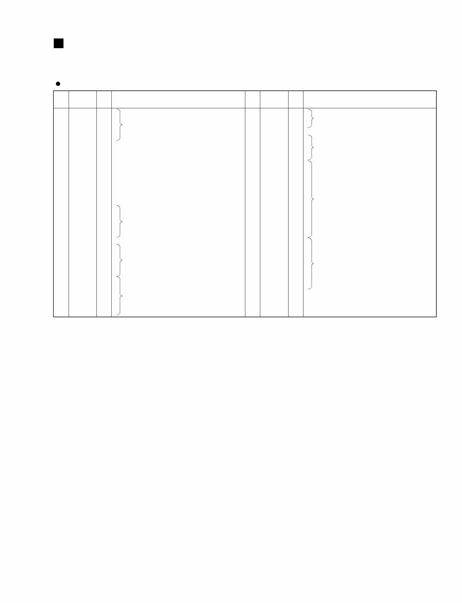
LSI PIN DESCRIPTION
PIN
NO.
I/O FUNCTION NAME
PIN
NO.
I/O FUNCTION NAME
1
2
3
4
5
6
7
8
9
10
11
12
13
14
15
16
17
18
19
20
21
22
23
24
25
26
27
28
29
30
31
32
S1
S2
S3
S4
S5
VREF+
VDD
OSC2
OSC1
VSS
XI
XO
MMOD
RD0
RXD
D0
D1
D2
D3
D4
/RST
D5
D6
D7
D8
D9
S6
S7
S8
S9
S10
S11
I
I
I
I
I
-
-
O
I
-
I
O
I
O
I
O
O
O
O
O
I
O
O
O
O
O
I
I
I
I
I
I
Switch matrix data
Power supply (+5V, analog)
Power supply (+5V)
Crystal oscillator (8MHz)
Crystal oscillator (8MHz)
Ground
Not used
Not used
Memory mode select (Grounded)
Rotary encoder data
MIDI receive data
LED and switch drive data
Reset
LED and switch drive data
Switch matrix data
33
34
35
36
37
38
39
40
41
42
43
44
45
46
47
48
49
50
51
52
53
54
55
56
57
58
59
60
61
62
63
64
S12
S13
S14
TXD
S15
S16
S17
S18
L16
L17
L18
L19
L8
L9
L10
L11
L12
L13
L14
L15
L7
L6
L5
L4
L3
L2
L1
L0
VREF
AD0
AD1
S0
I
I
I
O
I
I
I
I
O
O
O
O
O
O
O
O
O
O
O
O
O
O
O
O
O
O
O
O
-
I
I
I
Switch matrix data
MIDI transmit data
Switch matrix data
LED drive data
LED and switch drive data
Grounded
Analog input
Analog input
Switch matrix data
MN101C027YB (XS711200) CPU PN: IC001
EZ-AG
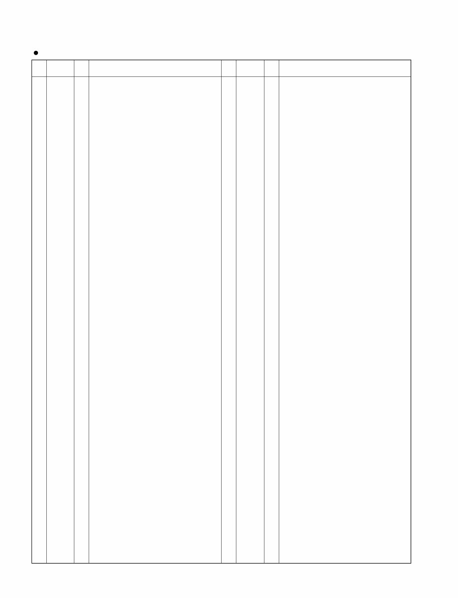
10
PIN
NO.
I/O FUNCTION NAME
PIN
NO.
I/O FUNCTION NAME
1
2
3
4
5
6
7
8
9
10
11
12
13
14
15
16
17
18
19
20
21
22
23
24
25
26
27
28
29
30
31
32
33
34
35
36
37
38
39
40
41
42
43
44
45
46
47
48
49
50
51
52
53
54
55
56
57
58
59
60
61
62
63
64
65
66
67
68
69
70
71
72
73
74
75
76
77
78
79
80
81
82
83
84
ICN
RFCLKI
TM2
AVDD_PLL
AVSS_PLL
MODE0
VCC7
GND8
XIN
XOUT
MODE1
TEST0
TESTON
AN0-P40
AN1-P41
AN2-P42
AN3-P43
AVDD_AN
AVSS_AN
TXD0
TXD1
EXCLK
SMD11
SMD4
SMD3
SMD12
SMD10
SMD5
SMD2
SMD13
SMD9
SMD6
SMD1
SMD14
VCC35
GND36
SMD8
SMD7
SMD0
SMD15
SOE
SWE
SRAS
SCAS
REFRESH
CS0
SMA0
SMA16
VCC49
GND50
SMA1
SMA15
SMA2
SMA14
SMA3
SMA13
SMA4
SMA12
SMA5
GND60
VCC61
SMA11
SMA6
SMA10
SMA7
SMA9
SMA17
SMA8
SMA18
SMA19
SMA20
SMA21
SMA22
SMA23
CMA20
CMA19
VCC77
GND78
CMA18
CMA17
CMA5
CMA6
CMA4
CMA7
I
I
I
I
I
O
I
I
I
I
I
I
I
O
O
O
I/O
I/O
I/O
I/O
I/O
I/O
I/O
I/O
I/O
I/O
I/O
I/O
I/O
I/O
I/O
I/O
O
O
O
O
O
O
O
O
O
O
O
O
O
O
O
O
O
O
O
O
O
O
O
O
O
O
O
O
O
O
O
O
O
O
O
O
O
O
O
Initial clear
PLL Clock
PLL Control
Power supply
Ground
SWX dual mode
Power supply
Ground
crystal oscillator
crystal oscillator
SWX separate mode
TEST pin
TEST pin
A/D converter
A/D converter
A/D converter
A/D converter
Power supply
Ground
for MIDI or TO-HOST
for MIDI
PORT-E2
Wave memory data bus
Wave memory data bus
Wave memory data bus
Wave memory data bus
Wave memory data bus
Wave memory data bus
Wave memory data bus
Wave memory data bus
Wave memory data bus
Wave memory data bus
Wave memory data bus
Wave memory data bus
Power supply
Ground
Wave memory data bus
Wave memory data bus
Wave memory data bus
Wave memory data bus
read signal
write signal
RAS signal
CAS signal
REFRESH signal
CS signal
Memory address bus
Memory address bus
Power supply
Ground
Memory address bus
Memory address bus
Memory address bus
Memory address bus
Memory address bus
Memory address bus
Memory address bus
Memory address bus
Memory address bus
Ground
Power supply
Memory address bus
Memory address bus
Memory address bus
Memory address bus
Memory address bus
Memory address bus
Memory address bus
Memory address bus
Memory address bus
Memory address bus
Memory address bus
Memory address bus
Memory address bus
Program address bus
Program address bus
Power supply
Ground
Program address bus
Program address bus
Program address bus
Program address bus
Program address bus
Program address bus
85
86
87
88
89
90
91
92
93
94
95
96
97
98
99
100
101
102
103
104
105
106
107
108
109
110
111
112
113
114
115
116
117
118
119
120
121
122
123
124
125
126
127
128
129
130
131
132
133
134
135
136
137
138
139
140
141
142
143
144
145
146
147
148
149
150
151
152
153
154
155
156
157
158
159
160
161
162
163
164
165
166
167
168
CMA3
CMA8
CMA2
CRD
CMA1
CUB
VCC91
GHND92
CS1
CMA0
CLB
CMA12
CMA11
CMA10
CMA9
GND100
CWE
CMA16
CMA15
CMA14
CMA13
CMD8
CMD7
CMD9
CMD6
CMD10
CMD5
CMD11
CMD4
CMD12
CMD3
CMD13
CMD2
CMD14
VCC119
GND115
CMD1
CMD15
CMD0
CMA21
PDT15
PDT14
PDT13
PDT12
PDT11
PDT10
PDT9
PDT8
VCC133
GND134
PDT7
PDT6
PDT5
PDT4
PDT3
PDT2
PDT1
PDT0
VCA143
GND144
PAD2
PAD1
PAD0
VCC148
GND149
PCS
PWR
PRD
RXD0
RXD1
SCLKI
ADIN
ADLR
DO0
DO1
SYSCLK
VCC161
GND162
WCLK
QCLK
BCLK
SYI
IRQ0
NMI
O
O
O
O
O
O
O
O
O
O
O
O
O
O
O
O
O
O
I/O
I/O
I/O
I/O
I/O
I/O
I/O
I/O
I/O
I/O
I/O
I/O
I/O
I/O
I/O
I/O
O
I/O
I/O
I/O
I/O
I/O
I/O
I/O
I/O
I/O
I/O
I/O
I/O
I/O
I/O
I/O
I/O
I
I
I
I
I
I
I
I
I
I
O
O
O
O
O
O
O
I
I
I
Program address bus
Program address bus
Program address bus
read signal
Program address bus
high byte effective signal
Power supply
Ground
CS signal
Program address bus
low byte effective signal
Program address bus
Program address bus
Program address bus
Program address bus
Ground
write signal
Program address bus
Program address bus
Program address bus
Program address bus
Program memory Data bus
Program memory Data bus
Program memory Data bus
Program memory Data bus
Program memory Data bus
Program memory Data bus
Program memory Data bus
Program memory Data bus
Program memory Data bus
Program memory Data bus
Program memory Data bus
Program memory Data bus
Program memory Data bus
Power supply
Ground
Program memory Data bus
Program memory Data bus
Program memory Data bus
Program address bus
SWX access data bus
SWX access data bus
SWX access data bus
SWX access data bus
SWX access data bus
SWX access data bus
SWX access data bus
SWX access data bus
Power supply
Ground
SWX access data bus
SWX access data bus
SWX access data bus
SWX access data bus
SWX access data bus
SWX access data bus
SWX access data bus
SWX access data bus
Power supply
Ground
SWX access address bus
SWX access address bus
SWX access address bus
Power supply
Ground
Chip select
write enable
read enable
for Midi or TO-HOST
for Midi or Key scan
EXT Clock
A/D converter
A/D converter LR clock
DAC
DAC
1/2 clock
Power supply
Ground
for DAC LR clock
1/12 clock
IIS-DAC clock
Synch signal
Interrupt request
Interrupt request
HG73C205AFD (XU947C00) SWX00B (Tone Generator) DM: IC101
You're Reading a Preview
What's Included?
Fast Download Speeds
Online & Offline Access
Access PDF Contents & Bookmarks
Full Search Facility
Print one or all pages of your manual
$30.99
Viewed 91 Times Today


Secure transaction
What's Included?
Fast Download Speeds
Online & Offline Access
Access PDF Contents & Bookmarks
Full Search Facility
Print one or all pages of your manual
$30.99
The YAMAHA EZ-AG Service Manual is a comprehensive guide for car repair, available in English. It comes in .PDF format, providing detailed technical information for both professional mechanics and DIY enthusiasts. This manual is an invaluable resource for anyone looking to perform maintenance, repairs, or troubleshooting on the YAMAHA EZ-AG.


