

VERTEX YAESU FT-817 Service Repair Manual
What's Included?
Fast Download Speeds
Online & Offline Access
Access PDF Contents & Bookmarks
Full Search Facility
Print one or all pages of your manual
©2003 VERTEX STANDARD CO., LTD. Printed in Japan.
(E137790A)
Technical Supplement
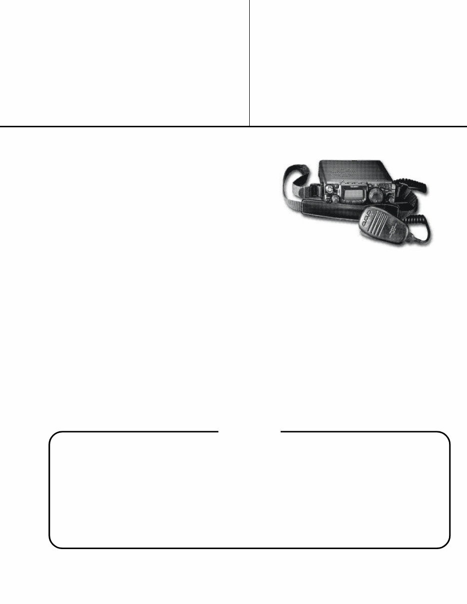
FT-817
HF / VHF / UHF
All Mode Transceiver
Introduction
This manual provides technical information necessary for
servicing the Yaesu FT-817 HF & V/UHF-Bands Trans-
ceiver. It does not include information on installation and
operation, which are described in the FT-817 Operating
Manual provided with the transceiver, or on accessories
which are described in their manuals.
The FT-817 is carefully designed to allow the knowledge-
able operator to make nearly all adjustments required for
various station conditions, modes and operator preferenc-
es simply from the controls on the panels, without open-
ing the case of the transceiver. The FT-817 Operating Man-
ual describes these adjustments, plus certain internal set-
tings.
Servicing this equipment requires expertise in handling
surface mount chip components. Attempts by unqualified
persons to service this equipment may result in perma-
nent damage not covered by warranty. For the major cir-
cuit boards, each side of the board is identified by the type
of the majority of components installed on that side. In
most cases one side has only chip components, and the
other has either a mixture of both chip and lead compo-
Contents
Specification .................................................. 2
Exploded View & Miscellaneous Parts ..... 3
Block Diagram ............................................... 5
Circuit Description ....................................... 7
Alignment ..................................................... 13
Interconnection Diagram ........................... 23
nents (trimmers, coils, electrolytic capacitors, packaged
ICs, etc.), or lead components only.
While we believe the technical information in this manu-
al is correct, VERTEX STANDARD assumes no liability
for damage that may occur as a result of typographical or
other errors that may be present. Your cooperation in
pointing out any inconsistencies in the technical informa-
tion would be appreciated. VERTEX STANDARD reserves
the right to make changes in this transceiver and the align-
ment procedures, in the interest of technological improve-
ment, without notification of owners.
Board Unit (Schematics, Layouts & Parts)
MAIN Unit ............................................................... 25
PLL Unit ................................................................... 57
REF Unit ................................................................... 65
PA / FINAL Unit ...................................................... 71
PANEL Unit ............................................................. 89
VR Unit ..................................................................... 99
TCXO-9 Unit (Option) .......................................... 100
VERTEX STANDARD CO., LTD.
4-8-8 Nakameguro, Meguro-Ku, Tokyo 153-8644, Japan
VERTEX STANDARD
US Headquarters
10900 Walker Street, Cypress, CA 90630, U.S.A.
International Division
8350 N.W. 52nd Terrace, Suite 201, Miami, FL 33166, U.S.A.
YAESU EUROPE B.V.
P.O. Box 75525, 1118 ZN Schiphol, The Netherlands
YAESU UK LTD.
Unit 12, Sun Valley Business Park, Winnall Close
Winchester, Hampshire, SO23 0LB, U.K.
VERTEX STANDARD HK LTD.
Unit 5, 20/F., Seaview Centre, 139-141 Hoi Bun Road,
Kwun Tong, Kowloon, Hong Kong

2
Specifications
General
Frequency Range:
Receive: 100 kHz-30 MHz
50 MHz-54 MHz
76 MHz-108 MHz (WFM only)
87.5 MHz-108 MHz (EU)
108 MHz-154 MHz (USA)
144 MHz-148 (146) MHz (Other markets)
430 (420) MHz-450 (440) MHz
Transmit:160-6 Meters
2 Meters
70 Centimeters (Amateur bands only)
5.1675 MHz Alaska Emergency Frequency
(USA only)
Emission Modes:
A1 (CW), A3 (AM), A3J (LSB/USB), F3 (FM),
F1 (9600 bps packet), F2 (1200 bps packet)
Synthesizer Steps (Min.):
10 Hz (CW/SSB), 100 Hz (AM/FM)
Antenna Impedance:
50 Ohms, Unbalanced (Front: Type BNC, Rear: Type M)
Operating Temp. Range:
–10 °C to +60 °C (+14 °F to +140 °F)
Frequency Stability:
±4 ppm from 1 min. to 60 min after power on.
@25 °C: 1 ppm/hour
±0.5 ppm/1 hour @25 °C, after warmup
(with optional TCXO-9)
Supply Voltage:
Normal: 13.8 VDC ± 15 %, Negative Ground
Operating: 8.0-16.0 V, Negative Ground
FBA-28 (w/8 “AA” Alkaline Cells): 12.0 V
FNB-72 (Ni-Cd Battery Pack): 9.6 V (Option)
Current Consumption:
Squelched: 250 mA (Approx.)
Receive: 450 mA
Transmit: 2.0 A
Case Size (W x H x D):
135 x 38 x 165 mm (5.31” x 1.5” x 6.50”)
Weight (Approx.):
1.17 kg (2.58 lb)
w/Alkaline battery, antenna, w/o Microphone
Transmitter
RF Power Output:
5 W (SSB/CW/FM), 1.5 W (AM Carrier) @13.8 V
Modulation Types:
SSB: Balanced Modulator
AM: Early Stage (Low Level)
FM: Variable Reactance
FM Maximum Deviation: ±5 kHz (FM-N: ±2.5 kHz)
Spurious Radiation: –50 dB (1.8-29.7 MHz)
–60 dB (50/144/430 MHz)
Carrier Suppression: >40 dB
Opp. Sideband Supp.: >50 dB
SSB Frequency Response: 400 Hz-2600 Hz (–6 dB)
Microphone Impedance:
200-10k Ohms (Nominal: 600 Ohms)
Receiver
Circuit Type: Double-Conversion Superheterodyne
Intermediate Frequencies:
1st: 68.33 MHz (SSB/CW/AM/FM); 10.7 MHz (WFM)
2nd: 455 kHz
Sensitivity: SSB/CW AM FM
100 kHz-500 kHz – – –
500 kHz-1.8 MHz – 32 μV –
1.8 MHz-28 MHz 0.25 μV 2 μV –
28 MHz-30 MHz 0.25 μV 2 μV 0.5 μV
50 MHz-54 MHz 0.2 μV 2 μV 0.32 μV
144/430 MHz 0.125 μV – 0.2 μV
(IPO, ATT off, SSB/CW/AM = 10 dB S/N, FM = 12 dB SINAD)
Squelch Sensitivity: SSB/CW/AM FM
1.8 MHz-28 MHz 2.5 μV –
28 MHz-30 MHz 2.5 μV 0.32 μV
50 MHz-54 MHz 1 μV 0.2 μV
144/430 MHz 0.5 μV 0.16 μV
(IPO, ATT off)
Image Rejection: HF/50 MHz: 70 dB
144/430 MHz: 60 dB
IF Rejection: 60 dB
Selectivity (–6/–60 dB):
SSB/CW: 2.2 kHz/4.5 kHz
AM: 6 kHz/20 kHz
FM: 15 kHz/30 kHz
FM-N: 9 kHz/25 kHz
SSB (optional YF-122S installed): 2.3 kHz/4.7 kHz (–66 dB)
CW (optional YF-122C installed): 500 Hz/2.0 kHz
AF Output: 1.0 W (8 Ohms, 10% THD or less)
AF Output Impedance: 4-16 Ohms
Specifications are subject to change without notice, and
are guaranteed within amateur bands only.
Frequency ranges vary according to transceiver version;
check with your dealer.
3
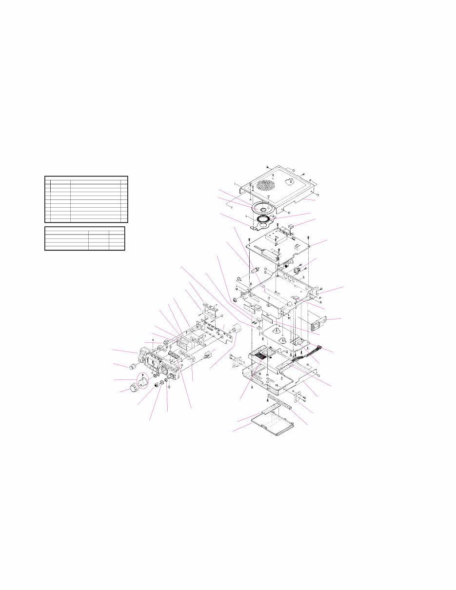
Exploded View & Miscellaneous Parts
RA026720B (Lot.36~)
RA026720A
CHASSIS
RA027660A
CONNECTOR COVER
CP6960001
TOP CASE ASS’Y (W/SP NET)
RA0270500
SP HOLDER
RA027150B (Lot.49~)
RA027150A
FRONT PANEL ASSY
RA0270300
RUBBER KNOB (ABC)
RA0270200
RUBBER KNOB (MODE)
RA0270100
RUBBER KNOB (CLAR)
RA027040A (Lot.35~)
RA0270400
RUBBER KNOB (PWR)
VR UNIT
RA026960A (Lot.54~)
RA0269600
ROTARY KNOB (SEL)
RA0269700
MAIN KNOB
RA0269800
RUBBER RING
RA0269400
ROTARY KNOB (AF)
RA0269500
ROTARY KNOB (SQL)
RA0276400 (X2 pcs)
BELT HOOK
RA027090A
BATTERY COVER
RA027080A
BOTTOM CASE
RA027530A
RELEASE KNOB (A)
MAIN UNIT
M4090150
SPEAKER
RA027540A
RELEASE KNOB (B)
RA027620B
COIL SPRING
(2 pcs)
RA0276300
HOLDER PLATE
PANEL UNIT
RA0271700
LCD HOLDER
Q7000291
LCD UNIT
RA027160A (Lot. 17~)
RA0271600
LIGHT GUIDE
RA0283600
REFLECTOR SHEET (A)
RA0289900
SPONGE RUBBER (BT-A)
RA0290000
SPONGE RUBBER (BT-B)
RA0293700
SPONGE RUBBER (CASE)
(Lot.23~ W/O CE)
RA0293600
PAD
RA0250800
PAD
RA0284300
SPONGE RUBBER (SH-B)
RA0284200 (X2 pcs)
SPONGE RUBBER (SH-A)
PA UNIT / FINAL UNIT
RA031630B (Lot.22~)
RA031630A (10~)
RA0316300 (8~)
RA0293500
SPONGE RUBBER (KEY-F)
RA0283900
SPONGE RUBBER (SP-B)
P1090352
CONNECTOR
P1091117A (Lot. 17~)
P1091117
CONNECTOR (w/ *1,*2)
RA0283800
SPONGE RUBBER (SP-A)
Q9000709A
ROTARY ENCODER
(W/ *3,*4)
ˆ
ˆ
ˆ
ˆ
˜
¨
¨
¨ ¨
¨
¨
ˆ
ˆ
˙
˙
¨
¨
AAB33X001
FBA-28
ˆ
`
¯
¯
¯
¯
¯ `
¯
¯
¯
¯
¯
¯
˘
˘
RA0283700
REFLECTOR SHEET (B)
R6054387B
SPECIAL NUT
´
*2
*1
*3
*4
No. VXSTD P/N Description Qty.
U9900112 TAPTITE SCREW M2X8B 1
U02308001 SEMS SCREW SM3X8 2
U04306002 SEMS SCREW HSM3X6NI 1
U20205007 BINDING HEAD SCREW M2.6X5B 7
U23206001 TAPTITE SCREW M2.6X6 1
U24205001 TAPTITE SCREW M2.6X5 11
U24306002 TAPTITE SCREW M3X6NI 2
U31204007 OVAL HEAD SCREW M2.6X4B 2
U31205007 OVAL HEAD SCREW M2.6X5B 8
U9900012 TAPTITE SCREW M2X4 2
Screw List
`
´
ˆ
˜
¯
˘
˙
¨
Description VXSTD P/N VERS.
ANTENNA (YHA-63) Q3000174
MIC (MH-31A8J) A06870001
CABLE (E-DC-6) Q9000722 W/O CE
DC CABLE (DC 3A 1500MM) T9023003 W/ CE
ACCESSORIES
4
Exploded View & Miscellaneous Parts
DESCRIPTION VALUE V/W TOL. VS P/N MFR’S DESIG VERS. REF. LOT. SIDE
*** MAIN ASSY ***
P 0004 WIRE ASSY J1012 to SP T9206744 1-
P 0005 WIRE ASSY J1008 to J4002 T9206919 1-
P 0006 WIRE ASSY J1003 to J3004 T9206920 1-
P 0007 WIRE ASSY BATTERY CASE T9206940 1-
P 0007 WIRE ASSY BATTERY CASE T9206932A 3-
5
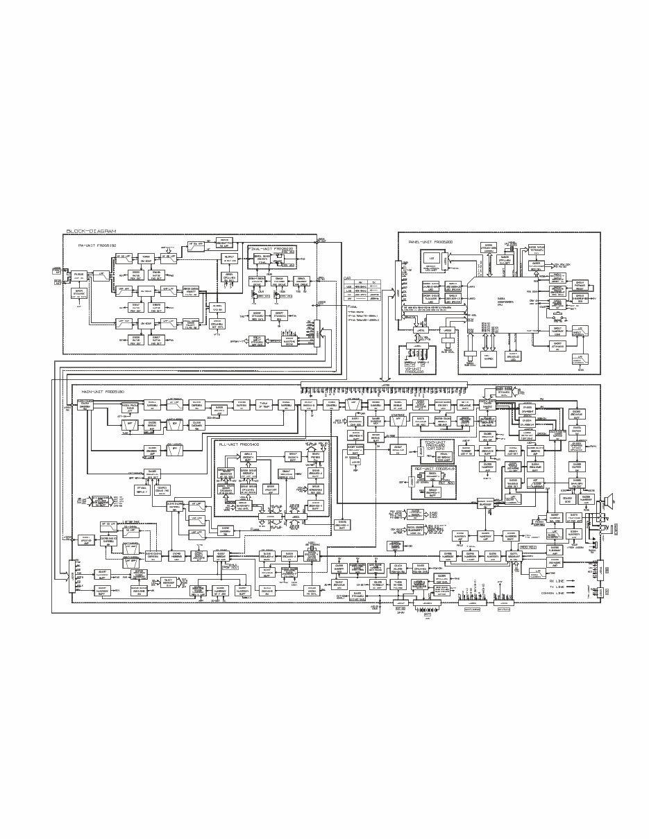
Block Diagram

6
Block Diagram
Note:

7
Circuit Description
The FT-817 internal assembly consists of the MAIN Unit,
Control ( PANEL) Unit, and the PA Unit. The MAIN Unit
contains the receiver front end, PLL IC, and switching cir-
cuits, as well as the VCO Unit (local oscillator for trans-
mission and reception). The PANEL Unit contains the
CPU and reset circuits, as well as the power circuitry for
the LCD.
Receive Signal Circuitry
High-Frequency Circuit
The receive signal enters from the Front (J1001) or Rear
(J1002) ANT connector , as selected by relay RL3016 on
the PA Unit.
Signals between 0.1 and 154 MHz received at the an-
tenna terminal pass through an input low-pass filter com-
posed of L3081, L3082, C3264, and C3265.
Received 430 MHz signals, after passing through a high-
pass filter composed of L3071, L3076, C3245, and C3254
are passed through low-pass filter composed of L3028,
L3032, L3035, C076, C3082, C3088, and C3093, and then
are fed through the directional coupler to the UHF T/R
switch circuit composed of diode switch D3004/D3035
(both HSU277). The signal then is fed to MAIN Unit via
J3002.
Received 145 MHz signals, after passing through a high-
pass filter composed of L3071, L3075, L3079, C3234, C3245,
C3252, and C3260 are passed through low-pass filter com-
posed of L3027, L3031, L3034, C3075, C3081, and C3092,
and then are fed through the directional coupler to the
VHF T/R switch circuit, composed of diode switch D3003/
D3005 (both HSU277) . The signal then is fed to MAIN
Unit via J3002.
Received 0.1-54 MHz signals, after passing through the
first low-pass filter, are passed through another low-pass
filter composed of L3069, L3070, L3074, L3077, C3239,
C3242, and C3248, plus LPFs 1-7 (5th or 7th-order
Chebyschev type filter) and HPFs 1-7, utilizing seven dif-
ferent sections to create optimized bandpass responses for
the various amateur bands at 0.1-54 MHz. The signal then
is fed to the 50MHz pre-amplifier (when engaged) and on
to the MAIN Unit via J3002.
The receive signal then passes through the input attenua-
tor (-10dB) which consists of resistors R1001, R1014, and
R1015 plus diodes D1003/D1011 (both DAP236U) on the
MAIN Unit .
Incoming wideband FM (76-108 MHz) signals, after pass-
ing through a high-pass filter composed of L3071, L3075,
L3079, C3234, C3245, C3252, and C3260 are passed
through a low-pass filter composed of L3027, L3031,
L3034, C3075, C3081, and C3092 , and through a direc-
tional coupler, to the VHF T/R switch circuit, composed
of diode switch D3003/D3005 (both HSU277) . Then it is
fed to the MAIN Unit via J3002. The signal is delivered to
IC Q1025 (CXA1611N) which contains the front-end and
discriminator circuits for Wide-FM demodulation. Then
the audio signal is passed to analog switch IC Q1049
(BU4066BF).
The FT-817 includes four receiver front ends, each opti-
mized for a particular frequency range and mode combi-
nation.
1st Mixer Circuit/1st IF Circuit
The 1st mixer on the MAIN Unit consists of a quad MES
FET, D1047 (GN2011). The 1st local signal (68.430-538.330
MHz) from the PLL Unit is applied to the gates of each
FET in the 1st mixer.
The resulting output signal (the difference between the
local signal and receive signal) passes through a mono-
lithic crystal filter (MCF) XF1001 (MF68R, BW:±7.5 kHz)
to obtain the 1st IF signal having a center frequency of
68.33 MHz. The signal is then fed to the 2nd mixer circuit
on the MAIN Unit after it is amplified by FET Q1051
(BB304C).
2nd Mixer Circuit/2nd IF Circuit
The 2nd mixer consists of FETs Q1060 and Q1062 (both
2SK302Y) on the MAIN Unit. The 2nd local signal (67.875
MHz) is amplified by Q1047 (2SC4154E) and is applied
to each FET's gate in the 2nd mixer.
The signal output from the 2nd mixer passes through a
ceramic filter, or optional mechanical filter (U1003), to
become the 455-kHz 3rd IF signal.
Noise Blanker Circuit
A sample of the 2nd IF circuit is amplified by FETs Q1052
and Q1061 (both BB301C) on the MAIN Unit, and then
is rectified by D1068 (1SS372). The resulting DC voltage
passes through R1343 and R1345, C1360 and C1362, and
Q1076 (2SC4154E) to yield an average AGC voltage for

8
Circuit Description
controlling the amplification gain of the above FETs. Noise
pulses contained in the output from D1075 are detected
by Q1074 (2SC4154E) and are used to control the NB Gate.
AGC Circuit
The AGC circuit consists of D1064 (1SS372), transistor
Q1066 (2SC4154E), and associated parts on the MAIN
Unit. Output from the AGC circuit is fed back to the RF
and IF stages, controlling their gain levels.
FM IF Circuit/FM Demodulator Circuit
The 2nd IF signal is fed to IC Q1069 (BA4116FV) for FM
demodulation.
The FM demodulator IC contains a mixer, limiter ampli-
fier, filter amplifier, squelch trigger, and demodulator. The
IF input signal is band-limited by ceramic filter CD1002
(CDBC455CX24, BW:±4 kHz), amplified by the limiter
amplifier, and demodulated into an audio signal by the
demodulator; it then passes through a filter (R1308 and
C1293). The signal next passes through a de-emphasis cir-
cuit which consists of R1256 and C1286.
The squelch circuit selectively amplifies the noise com-
ponent of the demodulator output using the filter ampli-
fier inside the FM IC and the active band-pass filter con-
sisting of an externally attached resistor and capacitor. This
circuit uses a signal detected by D1065 (DA221).
SSB/CW Demodulator Circuit
The 2nd IF signal is applied to the SSB demodulator Q1055
(SN16913) on the MAIN Unit, which produces audio by
applying a carrier signal from the CAR-DDS IC (Q1031).
Similarly, the CW signal is demodulated using a carrier
signal which is offset by the "Pitch" frequency.
The demodulated SSB and CW signals are each stripped
of high-frequency components by an active low-pass fil-
ter which consists of op-amp IC Q1093-1 (NJM2902V).
Then, they enter the VR Unit via J1008.
AM Demodulator Circuit
The 2nd IF signal from the IF Unit is applied to diode
D1060 (BAS316) for AM demodulation .
The output from the detector passes through analog switch
Q1049 (BU4066BF). Then, it enters the VR Unit via J1008.
Audio Amplifier Circuit
The demodulated signal that is selected by one of analog
switches IC Q1057 (according to the reception mode)
passes through the audio amplifier IC Q1094 (NJM2902V),
volume control VR4901, and IC Q1070 (TDA7233D) to
drive the internal or external speaker with a maximum
output of approximately 1.0 Watt.
Transmit Signal Circuitry
Microphone Amplifier Circuit
The audio signal from microphone jack J1014 on the
MAIN Unit is amplified by transistor Q1092 (2SC4154E)
on the MAIN Unit, and then is applied to electronic vol-
ume IC Q1071 (M62364EP), which is controlled via the
User Menu (Item #46: SSB MIC).
The output (audio signal) from the electronic volume IC
is amplified by Q1096 (NJM2902V) and fed to balanced
modulator IC Q1087 (SN16913) through the low-pass fil-
ter IC Q1096 (NJM2902V).
During FM transmission, the audio signal is adjusted via
the User Menu (Item# 29 : FM MIC) . The audio signal
that has passed through the pre-emphasis circuit (C2201
and R2228 on the MAIN Unit) may be mixed with a tone
signal from CPU IC Q4004, and is then amplified and lim-
ited by op-amp IC Q1095-4 (NJM2902V) of the IDC cir-
cuit. The audio then passes through the splatter filter (sec-
ondary active low-pass filter) formed by op-amp IC
Q1095-1 (NJM2902V), R1321, and R1322, plus C1344, and
is then fed to the frequency-modulator circuit on the
MAIN Unit through R1183 and R1477 for setting of the
frequency deviation.
SSB Modulator Circuit
The carrier signal appropriate to the transmitting mode
(LSB or USB) is applied from the CAR-DDS Unit to bal-
anced modulator IC Q1087 (SN16913) on the MAIN Unit,
and is modulated by microphone audio.
The balanced modulator produces the upper and lower
side bands and carrier signal. The carrier and audio sig-
nal are suppressed and the carrier balance is adjusted by
VR1001. As a result, the output signal obtained is a DSB
signal with a carrier suppression of 30 dB or more (addi-
tional carrier suppression is supplied by the SSB filter).
The DSB modulated signal (1st IF signal: 455 kHz) then
passes through ceramic filter CF1004 (CFJ455K14) or the
optional mechanical filter U1003 on the MAIN Unit, strip-
ping residual carrier and the undesired sideband; the sig-
nal then passes as an SSB signal through buffer-amplifier
Q1040 (BB301C).

9
Circuit Description
AM Modulator Circuit
As in the SSB modulator circuit, a carrier signal from the
CAR-DDS Unit and an audio signal from the microphone
are applied to balanced modulator IC Q1087 (SN16913)
on the MAIN Unit.
The control signal from MODE SW IC Q1021
(BU4094BCFV) on the MAIN Unit causes a voltage labeled
"AM 5V" to be sent from transistor Q1079 (2SC4154E). This
voltage is applied to IC Q1087 via D1077 (BAS316), caus-
ing the balanced modulator to lose balance. The restored
carrier signal and modulated signal are then fed to the Tx
mixer via ceramic filter CF1004 (CFJ455K14) on the MAIN
Unit.
Frequency Modulation Circuit
The FM circuit uses a voltage controlled crystal oscillator
(VCXO) which consists mainly of Q1033 (2SC4400),
X1001 on the MAIN-Unit, varactor diode D1056
(HVC362), and T1018. The VCXO has a center frequency
of 22.7785MHz.
The FM signal is produced by applying a signal from the
FM microphone amplifier circuit to varactor diode D1056
and varying the crystal oscillator load capacity in propor-
tion to the signal voltage.
CW (A1) Signal Generator Circuit
When the transmitting mode is CW (A1), the control sig-
nal from D-A converter IC Q1077 (M62353GP) on the
MAIN Unit creates a "CW 5V" voltage. The voltage is
applied to balanced modulator IC Q1087 via D1071, pro-
viding a carrier from the balanced modulator for the in-
put to the transmit signal circuit of the MAIN Unit.
1st IF Circuit/1st Mixer Circuit
The 455 kHz 1st IF signal from the modulator circuit is
band-limited by the MAIN Unit's ceramic (CF1004) or
optional mechanical filter U1003 (XF5201 or XF5301) ac-
cording to the selected mode (CW, SSB, or AM). It is then
buffer-amplified by FET Q1040 (BB301C) and fed to 1st
mixer IC Q1038 (SN16913).
The IF Unit's double balanced mixer IC Q1038 (DBM) is
used as the 1st mixer. A local signal (67.875MHz) is pro-
duced by tripling the Reference frequency at Q1047
(2SC4154E), and this local signal is fed to the "local" port
of the doubly-balanced mixer IC, where it is mixed with
the 455 kHz 1st IF signal to produce a 68.33MHz 2nd IF
signal.
2nd IF Circuit/2nd Mixer Circuit
The 2nd IF signal passes through crystal filter XF1001
and then is fed to the 2nd mixer circuit.
The 2nd mixer consists of the MAIN Unit's D1049
(HSB88WS). The 2nd local signal (68.430-538.330MHz)
from the PLL Unit is applied to the gates of each FET in
the 2nd mixer.
High-Frequency Transmit Preamplifier Circuit
The transmit signal is passed through a low-pass filter (1.8-
29.7 MHz), a high-pass filter (50-54 MHz), a band-pass
filter (144-146 MHz), or a band-pass filter (430-440 MHz)
and then is amplified by Q1001 (UPC2710), and passed
onward to the PA Unit via J1002.
Power Amplifier Circuit
The transmit signal from the MAIN Unit arrives at con-
nector J3001 on the PA Unit.
The transmit signal (1.8 MHz to 430 MHz) delivered to
the PA Unit is amplified by pre-driver Q3001 (2SC3357),
driver Q3002 (2SK5296) and final amplifiers Q5401/Q5402
(2SK2975).
Low-Pass Filter (LPF) Circuit
The transmission signal from the power amplifier circuit
is passed through a low-pass filter which consist mainly
of RL3001-RL3015, RL3017, and corresponding inductor
and capacitor networks. The LPF is a 5th or 7th-order
Chebyschev type filter, utilizing nine different sections for
the various amateur bands at 1.8 ~ 430 MHz.
The low-pass filtered transmission signal is fed to the
FRONT ANT connector (J0001) or REAR ANT connector
(J0002) through the triplexer and directional coupler.
The directional coupler samples a part of the transmis-
sion power to detect forward power and reflected power.
A DC voltage corresponding to the relative forward/re-
flected power is produced by D3032/D3033 (both MA716,
1.8 to 54 MHz), D3009/D3017 (both MA716, 144 to 148
MHz), or D3007/D3008 (both MA716, 430 to 450 MHz) ,
and is used for automatic level control (ALC).
ALC Circuit
The output from the directional coupler is routed from
connector J3004 and applied to the ALC circuit via con-
nector J1003 on the MAIN Unit.
The ALC circuit consists of an op-amplifier circuit for
amplifying the forward and reflected voltage, a time-con-

10
Circuit Description
stant ALC amplifier, and a transmit signal control circuit
on the MAIN Unit.
The forward voltage from connector J1003 on the MAIN
Unit is added with a DC control voltage and is then ap-
plied to op-amp IC Q1097 (NJM2902V).
The reflected voltage is added with a DC control voltage
and is then applied to op-amp IC Q1098 (NJM2904V), In
the event of high SWR conditions (SWR of 3:1 or more),
transmitter output is reduced and a "High SWR" warn-
ing appears, thus protecting the PA Unit from potential
damage and alerting the operator to the high SWR situa-
tion.
The ALC amplifier amplifies the "forward" DC output via
transistor Q1019 (2SC4154). This output then passes
through a fast-attack, slow-delay RC time-constant circuit
which consists of R1097 and C1113 for the input to the Tx
signal control circuit on the MAIN Unit.
The TX control circuit adjusts the IF amplifier gain via
gate 2 of FET Q1007 (BB304C) of the 68.33 MHz IF ampli-
fier circuit to prevent the power output from exceeding
the preset level.
PLL Frequency Synthesizer
The PLL Frequency Synthesizer consists mainly of a mas-
ter reference oscillator circuit, 2nd local oscillator circuit,
plus the PLL IC, CAR-DDS, and REF-DDS units, which
digitally synthesize carrier outputs, and a PLL circuit
which contains a voltage controlled oscillator (VCO).
Master Reference Oscillator Circuit
The master reference oscillator uses a crystal oscillator
(oscillation frequency: 22.625MHz) composed of Q5001
(2SC4400-4), X5001, TC5001, C5001, R5005, and associated
components. The reference oscillator signal passes through
buffer amplifier Q5002 (2SC4400-4), C5004, C5007, R5003,
R5004, R5007, and is then fed to the MAIN Unit via J5002.
CAR-DDS Circuit /REF-DDS Circuit
DDS ICs Q1031 (AD9835BRU) and Q2016 (AD9850BAS)
each contain a shift register, selector, phase accumulator,
and ROM.
The reference oscillation frequency (22.625MHz) that is
delivered to each of the DDS Units is applied to each DDS
IC after amplification by transistors Q1028/Q2020 (both
2SC4400-4).
The DDS outputs contain digital amplitude data corre-
sponding to serial frequency data from CPU IC Q4004 of
the PANEL Unit. The DDS frequency range is 453.5 ~ 466.5
kHz (cf = 455.0 kHz) for the CAR-DDS, and 7.2-8.0 MHz
for the REF DDS.
2nd Local Oscillator Circuit
The 2nd L.O. circuit is a Hartley-type overtone oscillator
circuit (frequency: 67.875 MHz) composed of Q1047
(2SC4400) on the MAIN Unit.
1st Local Oscillator Circuit
VCO output is buffer-amplified by Q2008 (2SC4400),
Q2011, Q2014, and Q2016(all 2SC5374) and passes
through a low-pass filter. It is then fed to the Tx/Rx fre-
quency mixer circuitry on the MAIN Unit.
PLL Circuit
The PLL circuit is a frequency mixing type composed of a
VCO, mixer, PLL IC, and loop filter.
The VCO consists of five circuits (VCO1, VCO2, VCO3,
VCO4, and VCO5), with a frequency range of 68.430-
538.330 MHz divided into five bands, allocated to the five
VCO circuits. VCO1-VCO5 consist mainly of FETs Q2004,
Q2005, and Q2006 (all 2SK210GR), transistors Q2009,
Q2010 (both 2SC5374), diodes D2001-D2006 (all HVC362),
D2007 (1SV282), D2008 (1SV281), and D2009 (1SV286), and
coils T2001-T2003, L2010, and L2011.
The VCO switching signal from connector J2002 is used
to drive switching transistors Q2001, Q2002, Q2003,
Q2012, and Q2013 (all DTC124EU) to switch the source
terminal of the oscillator FET.
The 68.430-538.330 MHz VCO signal is fed to mixer D1047
(GN2011-Q).
The REF-DDS signal (7.2-8.0 MHz) is fed to PLL IC Q2022
(FQ7925) after it passes through a LPF composed of C2064,
C2067, C2069, C2071, C2075, L2014, L2015, and L2016 ,
and buffer amplifier Q2019 (2SC4400-4) .
The phase of the reference frequency and that of the sig-
nal input to PLL IC are compared, and a signal whose
pulse corresponds to the phase difference is produced.
The VCO frequency is controlled by a first lag filter which
consists of R2057, R2065, R2062, and C2090 and a second-
ary lag filter composed of C2085, C2088, and R2053.
You're Reading a Preview
What's Included?
Fast Download Speeds
Online & Offline Access
Access PDF Contents & Bookmarks
Full Search Facility
Print one or all pages of your manual
$30.99
Viewed 28 Times Today


Secure transaction
What's Included?
Fast Download Speeds
Online & Offline Access
Access PDF Contents & Bookmarks
Full Search Facility
Print one or all pages of your manual
$30.99
This technical supplement includes a comprehensive range of content such as schematic diagrams, exploded parts diagrams, block diagrams, alignment procedures, board layouts, and more.
SUMMARY OF CONTENTS:
- Specifications: INCLUDED
- Exploded View & Miscellaneous Parts: INCLUDED
- Block Diagrams: INCLUDED
- Interconnection Diagram: INCLUDED
- Circuit Description: INCLUDED
- Parts List: INCLUDED
- Alignment Procedures: INCLUDED
- Board/Parts Layouts: INCLUDED
- Schematic Diagrams: INCLUDED
********************************
ABOUT THIS MANUAL
- PAGES: 102
- LANGUAGE: English
- PUBLICATION ID: E137790A
- PUBLICATION YEAR: 2003
- Has bookmarks for easy navigation: Yes
- Can be printed: Yes
- Windows compatible / Mac compatible
********************************
OUR GUARANTEE
- Every manual has been reviewed by humans for quality, correct number of pages, and bookmarks.
- The illustration above is a small preview from an actual screenshot of this manual.
Vertex Yaesu FT-817 Service Manual


