

VERTEX YAESU FT-8800 Service Repair Manual
What's Included?
Fast Download Speeds
Online & Offline Access
Access PDF Contents & Bookmarks
Full Search Facility
Print one or all pages of your manual
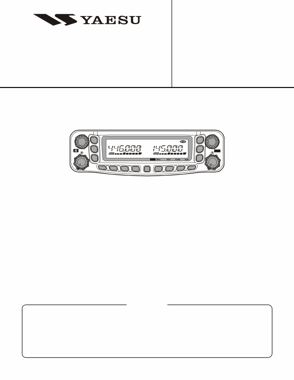
Dual Band FM Transceiver
FT-8800R
Technical Supplement
Introduction
This manual provides technical information necessary for servicing the FT-8800R Transceiver.
Servicing this equipment requires expertise in handling surface-mount chip components. Attempts by non-qualified
persons to service this equipment may result in permanent damage not covered by the warranty, and may be illegal in
some countries.
Two PCB layout diagrams are provided for each double-sided circuit board in the transceiver. Each side of thr board is
referred to by the type of the majority of components installed on that side (“leaded” or “chip-only”). In most cases one
side has only chip components, and the other has either a mixture of both chip and leaded components (trimmers, coils,
electrolytic capacitors, ICs, etc.), or leaded components only.
While we believe the technical information in this manual to be correct, Vertex Standard assumes no liability for dam-
age that may occur as a result of typographical or other errors that may be present. Your cooperation in pointing out any
inconsistencies in the technical information would be appreciated.
Specifications ..................................................... 2
Exploded View & Miscellaneous Parts ......... 3
Block Diagram .................................................... 5
Circuit Description ............................................ 7
Alignment ......................................................... 11
Contents
Board Unit (Schematics, Layouts & Parts)
Main Unit ...................................................................... 17
Panel Unit ..................................................................... 45
Panel-Sub Unit ............................................................. 51
VR-L Unit ...................................................................... 53
VR-R Unit ...................................................................... 54
© 2003 VERTEX STANDARD CO., LTD. (EH018M90A)
VERTEX STANDARD CO., LTD.
4-8-8 Nakameguro, Meguro-Ku, Tokyo 153-8644, Japan
VERTEX STANDARD
US Headquarters
10900 Walker Street, Cypress, CA 90630, U.S.A.
International Division
8350 N.W. 52nd Terrace, Suite 201, Miami, FL 33166, U.S.A.
YAESU EUROPE B.V.
P.O. Box 75525, 1118 ZN Schiphol, The Netherlands
YAESU UK LTD.
Unit 12, Sun Valley Business Park, Winnall Close
Winchester, Hampshire, SO23 0LB, U.K.
VERTEX STANDARD HK LTD.
Unit 5, 20/F., Seaview Centre, 139-141 Hoi Bun Road,
Kwun Tong, Kowloon, Hong Kong
1 4
6
5 2
3
LOW
SQL SQL
VOL VOL
LOW V/M HM
SCN
V/M HM SCN
KEY2
PWR

2
Specifications
GENERAL
Frequency Range: RX: 108.000 - 520.000 MHz,
700.000 - 999.995 MHz (Cellular Blocked)
TX: 144.000 - 146.000 MHz (or 144.000 - 148.000 MHz),
430.000 - 440.000 MHz (or 430.00 - 450.000 MHz)
Channel Steps: 5/10/12.5/15/20/25/50 kHz
Modes of Emission: F3, F2
Antenna Impedance: 50-Ohms, unbalanced (Antenna Duplexer built-in)
Frequency Stability: ±5 ppm @ 14° F ~ +140° F (–10 °C ~ +60 °C)
Operating Temperature Range: –4° F ~ +140° F (–20 °C ~ +60 °C)
Supply Voltage: 13.8 VDC (±15%), negative ground
Current Consumption (Approx.): RX: 0.5 A (Squelched)
TX: 8.5 A (144 MHz), 8.0 A (430 MHz)
Case Size (W x H x D): 5.5” x 1.6” x 6.6” (140 x 41.5 x 168 mm) (w/o knobs & connectors)
Weight (Approx.): 2.2 lb (1 kg)
TRANSMITTER
Output Power: 50/20/10/5 W (144 MHz),
35/20/10/5 W (430 MHz)
Modulation Type: Variable Reactance
Maximum Deviation: ±5 kHz
Spurious Radiation: Better than –60 dB
Microphone Impedance: 2 kΩ
DATA Jack Impedance: 10 kΩ
RECEIVER
Circuit Type: Double-conversion superheterodyne
Intermediate Frequencies: 45.05 MHz/450 kHz (Main band),
47.25 MHz/450 kHz (Sub band)
Sensitivity (for 12dB SINAD): Better than 0.2 µV
Squelch Sensitivity: Better than 0.16 µV
Selectivity (–6dB/–60dB): 8 kHz/30 kHz
Maximum AF Output: 2 W @ 8 Ω for 5% THD
AF Output Impedance: 4-16 Ω
Specifications are subject to change without notice, and are guaranteed within the 144 and 430 MHz amateur bands only. Frequen-
cy ranges will vary according to transceiver version; check with your dealer.
3
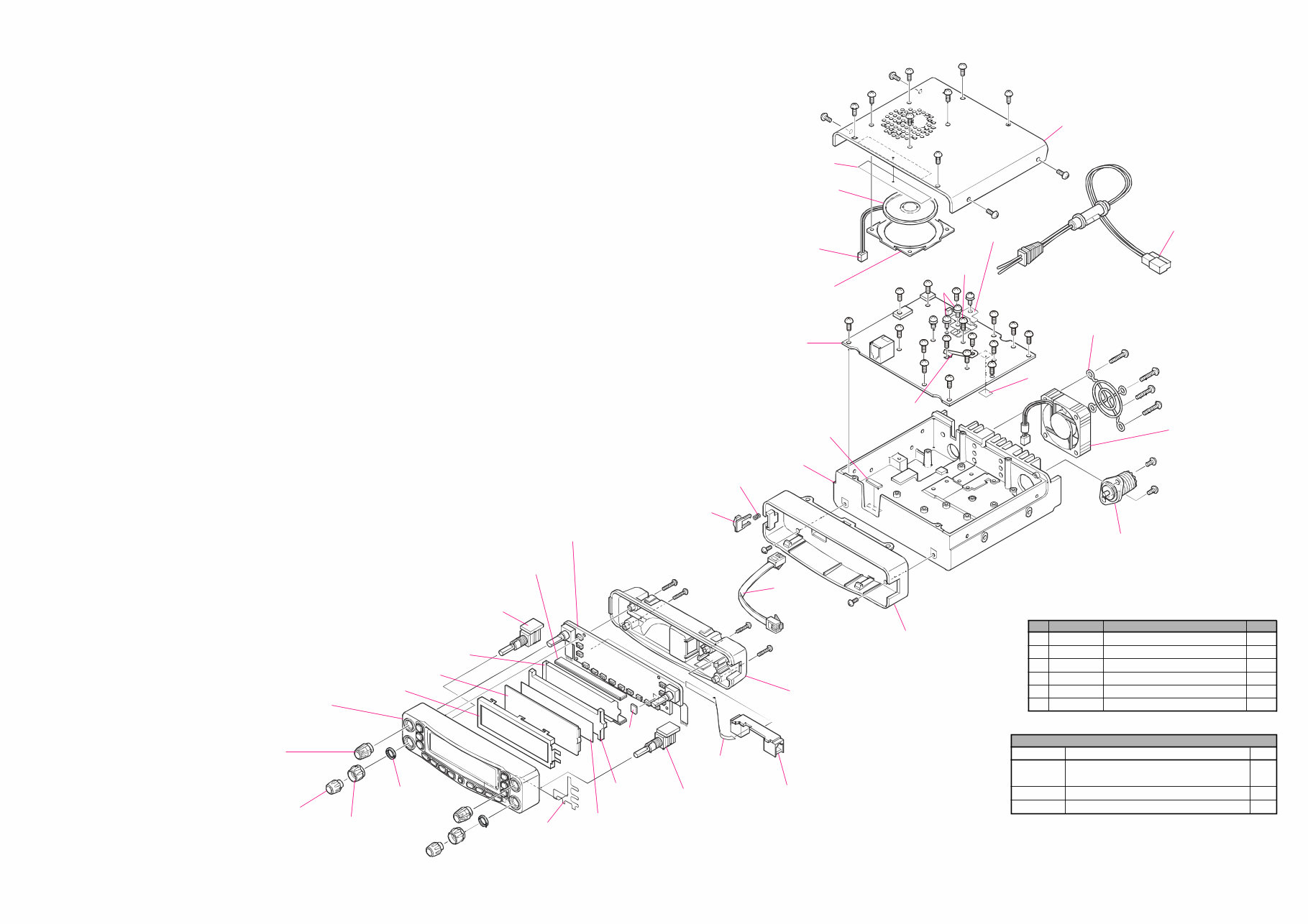
Exploded View & Miscellaneous Parts
RA0396700
LIGHT GUIDE
RA0396800
LCD HOLDER
RA0396900 (x2 pcs)
INTER CONNECTOR
RA0397100
REFLECTOR SHEET
RA0397000
DIFFUSER SHEET
M2090034A
FAN
M4090149
SPEAKER
RA0404400 (x2 pcs)
KNOB
RA0404300 (x2 pcs)
KNOB
RA0404200 (x2 pcs)
ENCODER KNOB
R6054387B (x2 pcs)
SPECIAL NUT
RA0507300
FRONT PANEL ASSY
RA0407200
SPACER
T9207010A
WIRE ASSY
RA040710A
LIGHT SHEET
T9206438A
WIRE ASSY
R0150630
HOLDER
RA02132A0
HIMERON TAPE
CS1770001
CASE (W/O NYLON NET)
T9206228
WIRE ASSY
RA040480A
SUB PANEL ASSY
(W/ COIL SPRING, RELEASE KNOB)
T9101509
CT CABLE
S5000206
FAN GUARD
P1090984
CONNECTOR
RA0446200
LEAF SPRING
RA0396100
REAR PANEL
RA02668AA
CHASSIS
RA0441300
PAD
RA0438700
RUBBER
G6090147A
LCD
VR-L Unit
VR-R UNIT
PANEL Unit
PANEL-SUB UNIT
MAIN UNIT
RA0415200 (x2 pcs)
GROUND PLATE
R0137550
COIL SPRING
RA026900A
RELEASE KNOB
No. VXSTD P/N DESCRIPTION QTY.
U23116007 TAPTITE SCREW M2X16B 4
U31206007 OVAL HEAD SCREW M2.6X6B 14
U44308002 TAPTITE SCREW M3X8NI 17
U03310002 SEMS SCREW ASM3X10NI 4
U20308002 BINDING HEAD SCREW M3X8NI 2
U20318007 BINDING HEAD SCREW M3X18B 4
Non-designated parts are available only
as part of a designated assembly.
SUPPLIED ACCESSORIES
VXSTD P/N DESCRIPTION QTY.
AAA43X001 MH-48
A6J
1
A07530005 MH-42
B6JS
(depending on transceiver version)
T9021715 DC POWER CORD W/FUSE 1
Q0000081 SPARE FUSE 15 A 2

4
Exploded View & Miscellaneous Parts
Note:
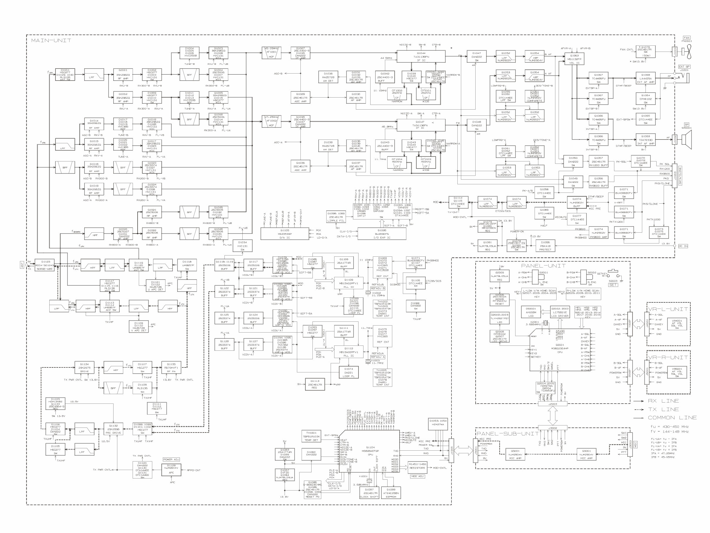
Block Diagram
5

Block Diagram
6
Note:

7
Circuit Description
Receiver Signal Path
“Main” Band 430 MHz Signal
The 430 MHz signal is passed through a high-pass filter
network and a low-pass filter network to the antenna
switch diodes D1029, D1030 (both RSL135) and D1001
(HSC277TRF), then passed through another low-pass fil-
ter network to the “Main” band RF amplifier Q1001
(3SK296ZQ).
The amplified 430 MHz signal is passed through the band
switch D1002 (HSC277) to the varactor-tuned band-pass
filter network consisting of D1004, D1005, and D1006 (all
HVC350B) and associated circuitry, then applied to the
first mixer Q1003 (3SK296ZQ). Meanwhile, the UHF lo-
cal signal from the UHF-VCO/B Q1116 (2SC5006) is de-
livered to first mixer Q1003, yielding the 45.05 MHz
“Main” band first IF.
“Main” Band 144 MHz Signal
The 144 MHz signal is passed through a low-pass filter
network and a high-pass filter network to the antenna
switch diodes D1113, D1114 (both UM9957F), D1115,
D1116 (both RLS135) and D1117 (both RLS135) then
passed through another low-pass filter network to the
“Main” band RF amplifier Q1014 (3SK296ZQ).
The amplified 144 MHz signal is passed through a varac-
tor-tuned band-pass filter network consisting of D1017,
D1018, D1019 (all HVC365) and associated circuitry to
the first mixer Q1016 (3SK296ZQ). Meanwhile, the VHF
local signal from the VHF-VCO/B Q1120 (2SC5374) is
delivered to first mixer Q1016, yielding the 45.05 MHz
“Main” band first IF.
“Main” Band IF and AF Signals
The 45.05 MHz “Main” band first local signal is delivered
to the monolithic crystal filter XF1001 which strips away
unwanted mixer products, then is passed through IF am-
plifier Q1027 (2SC4400) to the IF IC Q1044 (TA31136FN).
Meanwhile, a portion of the output of 11.15 MHz crystal
X1002 is multiplied fourfold by Q1042 (2SC4400) to pro-
vide the 44.6 MHz second local signal, then delivered to
the IF IC Q1044. Within the IF IC Q1044, the 44.6 MHz
second local signal is mixed with the 45.05 MHz “Main”
band first local signal to produce the 450 kHz “Main” band
second IF.
The 450 kHz “Main” band second IF is passed through
the filter switch D1039/D1041 (both HSC277) to the ce-
ramic filter CF1001 (CFWM450E) which strips away all
but the desired signal, then it passes through the IF am-
plifier within Q1044 to the ceramic discriminator CD1001
(CDBM450C24), which removes any amplitude variations
in the 450 kHz IF signal before detection of speech.
The demodulated “Main” band audio is passed through
the de-emphasis network, audio switch D1047 (DAN222),
low-pass filter network (consisting of Q1052 (NJM2902V)
and associated circuitry), and a high-pass filter network
(consisting of Q1054 (NJM2904V) and associated circuit-
ry). The filtered audio signal is passed through the audio
volume control IC Q1063 (M51132FP), which adjusts the
audio sensitivity to compensate for audio level variations,
then is delivered to the audio switch Q1066 and Q1067
(both TC4W66FU).
When the internal speaker is selected, the audio signal is
amplified by Q1069 (TDA7233D) then applied to the in-
ternal loudspeaker. When the external speaker is select-
ed, the audio signal is amplified by Q1068 (LA4425A),
then it passes through the EXT SP jack to the external loud-
speaker.
“Sub” Band 430 MHz Signal
The 430 MHz signal is passed through a high-pass filter
network and a low-pass filter network to the antenna
switch diodes D1029, D1030 (both RSL135) and D1001
(HSC277TRF), then passed through another low-pass fil-
ter network to the “Sub” band RF amplifier Q1002
(3SK296ZQ).
The amplified 430 MHz signal is delivered through the
band switch D1009 (HSC277) to the varactor-tuned band-
pass filter network consisting of D1011, D1012, D1013 (all
HVC350B) and associated circuitry, then applied to the
first mixer Q1005 (3SK296ZQ). Meanwhile, the UHF lo-
cal signal from the UHF-VCO/A Q1123 (2SC5006) is de-
livered to first mixer Q1005, yielding the 47.25 MHz “Sub”
band first IF.
“Sub” Band 144 MHz Signal
The 144 MHz signal is passed through a low-pass filter
network and a high-pass filter network to the antenna
switc diodes D1113, D1114 (both UM9957F), D1115,
D1116 (both RLS135) and D1117 (both RLS135), then
passed through another low-pass filter network to the
“Sub” band RF amplifier Q1015 (3SK296ZQ).
The amplified 144 MHz signal is passed through the var-
actor-tuned band-pass filter network consisting of D1020,
D1021, D1022 (all HVC365) and associated circuitry to
the first mixer Q1017 (3SK296ZQ). Meanwhile, the VHF
local signal from the VHF-VCO/A Q1126 (2SC5374) is
delivered to first mixer Q1017, yielding the 47.25 MHz
“Sub” band first IF.
“Sub” Band IF and AF Signal
The 47.25 MHz “Sub” band first IF is delivered to the
monolithic crystal filter XF1002 which strips away un-
wanted mixer products, then passed through the IF am-
plifier Q1035 (2SC4400) to the IF IC Q1047 (TA31136FN).

8
Meanwhile, a portion of the output of 11.7 MHz crystal
X1003 is multiplied fourfold by Q1043 (2SC4400) to pro-
vide the 46.8 MHz second local signal, then applied to the
IF IC Q1047. Within the IF IC Q1047, the 46.8 MHz second
local signal is mixed with the 47.25 MHz “Sub” band first
local signal to produce the 450 kHz “Sub” band second IF.
The 450 kHz “Sub” band second IF is delivered to the
ceramic filter CF1003 (CFWM450E) which strips away all
but the desired signal, then passed through the IF ampli-
fier within Q1047 to the ceramic discriminator CD1002
(CDBM450C24) which removes any amplitude variations
in the 450 kHz IF signal before detection of speech.
The demodulated “Sub” band audio is passed through the
de-emphasis network, audio switch D1048 (DAN222),
low-pass filter network (consisting of Q1053 (NJM2902V)
and associated circuitry) and the high-pass filter network
(consisting of Q1054 (NJM2904V) and associated circuit-
ry). The filtered audio signal is passed through the audio
volume control IC Q1063 (M511312FP), which adjusts the
audio sensitivity to compensate for audio level variations,
then is delivered to the audio switch Q1066 and Q1067
(both TC4W66FU).
When the internal speaker is selected, the audio signal is
amplified by Q1069 (TDA7233D) then applied to the in-
ternal loudspeaker. When the external speaker is select-
ed, the audio signal is amplified by Q1068 (LA4425A),
then it passes through the EXT SP jack to the external loud-
speaker.
Squelch Control
“Main” Band
When no carrier is being received on the “Main” band,
noise at the output of the detector stage in Q1044 is am-
plified and band-pass filtered by the noise amp section of
Q1044. The resulting DC voltage is delivered to pin 5 of
main CPU Q1104 (M38268MCL), which compares the
squelch threshold level to that which set by the front pan-
el SQL knob.
While no carrier is being received on the “Main” band,
pin 2 of Q1105 remain “low,” to disable the audio output
from the speaker.
“Sub” Band
When no carrier is being received on the “Sub” band, noise
at the output of the detector stage in Q1047 is amplified
and band-pass filtered by the noise amp section of Q1047.
The resulting DC voltage is delivered to pin 2 of main
CPU Q1104, which compares the squelch threshold level
to that which set by the front panel SQL knob.
While no carrier is being received on the “Right” band,
pin 15 of Q1105 remain “low,” to disable the audio out-
put from the speaker.
Transmitter Signal Path
AF Signal
The speech signal from the microphone is passed through
the MIC jack J3003 to the AF amplifier Q3001 (NJM2904V)
on the PANEL-SUB UNT. The amplified speech signal is
passed through the panel separation jacks J3001 and J1005
to the MAIN Unit. On the MAIN UNIT, the speech signal
is delivered to the limiting amplifier Q1074 (NJM2902V) to
prevent over-modulation, then is delivered to a low-pass
filter network consisting of Q1074 and associated circuitry.
430 MHz Signal
The adjusted speech signal from Q1074 is passed through
transistor switch Q1114, Q1115 (both DTC144EE) to var-
actor diodes D1079 (HVC375B) and D1080 (HVC350B),
which frequency modulate the transmitting VCO, made
up of UHF-VCO/B Q1116 ( 2SC5006 ) and D1081
(HSC277).
The modulated transmit signal is passed through buffer
amplifiers Q1117, Q1118 and Q1119 (all 2SC5006) and
diode switches D1099, D1101 (both HSC277) to the pre-
drive amplifier Q1132 (2SK2596).
The amplified transmit signal from Q1132 is passed
through diode switch D1106 (HSC277) and the driver am-
plifier Q1134 (RD07MVS1) to the diode switch D1107
(HSC277), then finally amplified by power amplifier
Q1135 (RD70HVF1), providing up to 35 Watts of power
output. These three stages of the power amplifier’s gain
are controlled by the APC circuit.
The 35-Watt RF signal is passed through a high-pass fil-
ter network to the antenna switch D1118, D1119, and
D1120 (all UM9957F), then passed through a low-pass
filter network and another high-pass filter network to the
ANT jack.
144 MHz Signal
The adjusted speech signal from Q1074 is passed through
the transistor switch Q1114, Q1115 (both DTC144EE) to
varactor diodes D1082 and D1085 (both HVC365), which
frequency modulate the transmitting VCO, made up of
VHF-VCO/B Q1120 (2SC5374) and D1083 (HVC131).
The modulated transmit signal is passed through buffer
amplifiers Q1121 and Q1122 (both 2SC5374) and diode
switches D1089 and D1102 (both HSC277) to the pre-drive
amplifier Q1132 (2SK2596).
The amplified transmit signal from Q1132 is passed
through the diode switch D1105, D1106 (both HSC277)
and the driver amplifier Q1134 (RD07MVS1) to diode
switch D1108 (RLS135), then finally amplified by power
amplifier Q1135 (RD70HVF1) up to 50 Watts of power
output. These three stages of the power amplifier’s gain
are controlled by the APC circuit.
Circuit Description

9
The 50-Watt RF signal is passed through a low-pass filter
network to the antenna switch D1113 and D1114
(UM9957F), then passed through a high-pass filter net-
work and another low-pass filter network to the ANT jack.
APC (Automatic Power Control) Circuit
430 MHz
A portion of the power amplifier output is rectified by
D1121 and D1122 (both MA2S728) then delivered to APC
Q1129 (NJM2904V), as a DC voltage which is proportional
to the output level of the power amplifier.
At Q1129, the rectified DC voltage from the power am-
plifier is compared to the reference voltage from the main
CPU Q1104 to produce a control voltage, which regulates
the supply voltage to the pre-drive amplifier Q1132
(2SK2596), driver amplifier Q1134 (RD07MVS1), and
power amplifier Q1135 (RD70HVF1), so as to maintain
stable output power under varying antenna loading con-
ditions.
144 MHz
A portion of the power amplifier output is rectified by
D1109 and D1110 (both MA2S728) then delivered to APC
Q1129 (NJM2904V), as a DC voltage which is proportional
to the output level of the power amplifier.
At Q1129, the rectified DC voltage from the power am-
plifier is compared to the reference voltage from the main
CPU Q1104 to produce a control voltage, which regulates
the supply voltage to the pre-drive amplifier Q1132
(2SK2596), driver amplifier Q1134 (RD07MVS1), and
power amplifier Q1135 (RD70HVF1), so as to maintain
stable output power under varying antenna loading con-
ditions.
PTT (Push to Talk) Circuit
430 MHz
When the PTT switch is pressed, pin 8 of sub CPU Q2001
(M38223M4M) goes “high,” which sends the “PTT” com-
mand to main CPU Q1104.
When the “PTT” command is received, the main CPU
controls the I/O IC Q1095 (BU2090FS), causing pin 8 of
Q1095 to go “low” which activates the UHF TX switch
section of Q1096 (IMT17).
When the UHF TX switch section of Q1096 is activated, it
controls the antenna switch diodes D1118, D1119, and
D1120 (all UM9957F), modulator switching diode D1088
(DAN222), modulator switching transistor Q1114 and
Q1115 (both DTC144EE), diode switches D1099, D1101,
D1106 and D1107 (all HSC277), and APC switches Q1130
(DTA144EE) and Q1131 (DTC144EE), which activate the
430 MHz transmitter circuit.
144 MHz
When the PTT switch is pressed, pin 8 of sub CPU Q2001
(M38223M4M) goes “high,” which sends the “PTT” com-
mand to main CPU Q1104.
When the “PTT” command is received, the main CPU
controls the I/O IC Q1095 (BU2090FS), causing pin 9 of
Q1095 to go “low” which activates the VHF TX switch
section of Q1096 (IMT17).
When the VHF TX switch section of Q1096 is activated, it
controls the antenna switch diodes D1113 and D1114
(both UM9957F), D1117 (HSC277) and D1115, D1116
(RLS135), modulator switching transistor Q1114 and
Q1115 (both DTC144EE), diode switches D1089, D1102,
D1105, D1106 (all HSC277) and D1108 (RLS135), and APC
switches Q1130 (DTA144EE) and Q1131 (DTC144EE),
which activate the 144 MHz transmitter circuit.
PLL Circuit
“Main” band
A portion of the output from UHF-VCO/B Q1116
(2SC5006) is passed through buffer amplifier Q1117
(2SC5006) and diode switch D1086 (HSC277) to the pro-
grammable divider section of the PLL IC Q1109
(MB15A02PFV1), where it is divided according to the fre-
quency dividing data associated with the operating fre-
quency input from the main CPU Q1104. It is then sent to
the phase comparator.
A portion of the output from the VHF-VCO/B Q1120
(2SC5374) is passed through buffer amplifier Q1121
(2SC5374) and diode switch D1087 (HSC277) to the pro-
grammable divider section of the PLL IC Q1109, where it
is divided according to the frequency dividing data asso-
ciated with the operating frequency input from the main
CPU Q1104. It is then sent to the phase comparator.
The 11.15 MHz reference oscillator X1002 frequency is di-
vided by the reference frequency divider section of Q1109
into 2230 or 1784 parts, to become 5 kHz or 6.25 kHz com-
parative reference frequencies, which are utilized by the
phase comparator.
The phase comparator section of Q1109 compares the
phase between the frequency-divided oscillation frequen-
cy of the VCO circuit and the comparative frequency, and
its output is a pulse corresponding to the phase differ-
ence. This pulse is integrated by the loop filter into a con-
trol voltage (VCV) to control the oscillation frequency of
the VCOs.
Circuit Description

10
“Sub” band
A portion of the output from the UHF-VCO/A Q1123
(2SC5006) is passed through buffer amplifier Q1124
(2SC5006) and diode switch D1093 (HVC131) to the pro-
grammable divider section of the PLL IC Q1122
(MB15A02PFV1), where it is divided according to the fre-
quency dividing data associated with the operating fre-
quency input from the main CPU Q1104. It is then sent to
the phase comparator.
A portion of the output from the VHF-VCO/A Q1126
(2SC5374) is passed through buffer amplifier Q1127
(2SC5374) and diode switch D1097 (HVC131) to the pro-
grammable divider section of the PLL IC Q1122, where it
is divided according to the frequency dividing data asso-
ciated with the operating frequency input from the main
CPU Q1104. It is then sent to the phase comparator.
The 11.7 MHz reference oscillator X1003 frequency is di-
vided by the reference frequency divider section of Q1122
into 2340 or 1872 parts to become 5 kHz or 6.25 kHz com-
parative reference frequencies, which are utilized by the
phase comparator.
The phase comparator section of Q1122 compares the
phase between the frequency-divided oscillation frequen-
cy of the VCO circuit and the comparative frequency, and
its output is a pulse corresponding to the phase differ-
ence. This pulse is integrated by the loop filter into a con-
trol voltage (VCV) to control the oscillation frequency of
the VCOs.
Circuit Description
Power Supply Line
When the user presses and holds in the “Right” VOL knob
for 2 seconds, pin 23 of the main CPU Q1104 goes “low”
and pin 40 of main CPU Q1104 goes “high,” which acti-
vates the power switch Q1078 (2SB1301) and Q1082
(2SC4617), to supply 13.8 VDC to each circuit in the trans-
ceiver.
You're Reading a Preview
What's Included?
Fast Download Speeds
Online & Offline Access
Access PDF Contents & Bookmarks
Full Search Facility
Print one or all pages of your manual
$30.99
Viewed 97 Times Today


Secure transaction
What's Included?
Fast Download Speeds
Online & Offline Access
Access PDF Contents & Bookmarks
Full Search Facility
Print one or all pages of your manual
$30.99
This manual includes schematic diagrams, block diagrams, exploded views, alignment procedures, board layouts, and more. It provides a small preview of the schematic diagram for reference. The manual has bookmarks for easy navigation and can be printed. It is compatible with both Windows and Mac operating systems.
Details:
- Pages: 48
- Language: English
- Publication ID: EH018M90A
- Publication Year: 2003
Contents:
- Specifications
- Exploded Views
- Block Diagrams
- Circuit Description
- Parts List
- Alignment Procedures
- Board/Parts Layouts
- Schematic Diagrams
This is the Vertex-Yaesu FT-8800 Service Manual. For more high-quality manuals, please visit the provided link.


