


SERVICE
MANUAL
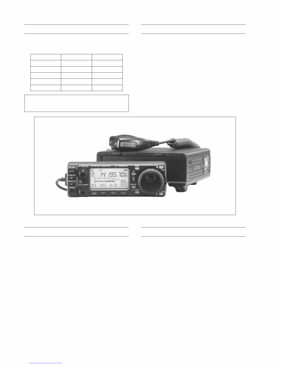
HF/VHF/UHF ALL MODE TRANSCEIVER
i706MK™G
Downloaded from www.Manualslib.com manuals search engine
INTRODUCTION
This service manual describes the latest service information
for the IC-706MKIIG HF/VHF/UHF ALL MODE TRANS-
CEIVER at the time of publication.
To upgrade quality, any electrical or mechanical parts and
internal circuits are subject to change without notice or
obligation.
DANGER
NEVER connect the transceiver to an AC outlet or to a DC
power supply that uses more than 16 V. This will ruin the
transceiver.
DO NOT expose the transceiver to rain, snow or any liquids.
DO NOT reverse the polarities of the power supply when con-
necting the transceiver.
DO NOT apply an RF signal of more than 20 dBm (100 mW)
to the antenna connector. This could damage the trans-
ceiver’s front end.
ORDERING PARTS
Be sure to include the following four points when ordering
replacement parts:
1. 10-digit order numbers
2. Component part number and name
3. Equipment model name and unit name
4. Quantity required
<SAMPLE ORDER>
1110004080 S.IC μPC2709T IC-706MKIIG MAIN UNIT 05 pieces
8810009020 Screw FH M2.6 x 5 ZK IC-706MKIIG Top cover 10 pieces
Addresses are provided on the inside back cover for your
convenience.
REPAIR NOTES
1. Make sure a problem is internal before disassembling the
transceiver.
2. DO NOT open the transceiver until the transceiver is
disconnected from its power source.
3. DO NOT force any of the variable components. Turn
them slowly and smoothly.
4. DO NOT short any circuits or electronic parts. An insu-
lated tuning tool MUST be used for all adjustments.
5. DO NOT keep power ON for a long time when the trans-
ceiver is defective.
6. DO NOT transmit power into a signal generator or a
sweep generator.
7. ALWAYS connect a 50 dB to 60 dB attenuator between
the transceiver and a deviation meter or spectrum ana-
lyzer when using such test equipment.
8. READ the instructions of test equipment thoroughly
before connecting equipment to the transceiver.
VERSION NO.
#02, #12
#03, #13
#04, #14
#05, #15
#08, #18
VERSION
Europe
France
Spain
U.S.A.
Other
SYMBOL
EUR
FRA
ESP
USA
OTH
Downloaded from www.Manualslib.com manuals search engine

TABLE OF CONTENTS
SECTION 1 SPECIFICATIONS
SECTION 2 INSIDE VIEWS
SECTION 3 CIRCUIT DESCRIPTION
3 - 1 RECEIVER CIRCUITS ................................................................................................................................ 3 - 1
3 - 2 TRANSMITTER CIRCUITS......................................................................................................................... 3 - 4
3 - 3 PLL CIRCUITS ............................................................................................................................................ 3 - 6
3 - 4 LOGIC CIRCUITS ....................................................................................................................................... 3 - 8
SECTION 4 ADJUSTMENT PROCEDURES
4 - 1 PREPARATION BEFORE SERVICING ...................................................................................................... 4 - 1
4 - 2 PLL ADJUSTMENTS................................................................................................................................... 4 - 2
4 - 3 TRANSMITTER ADJUSTMENTS ............................................................................................................... 4 - 2
4 - 4 RECEIVER ADJUSTMENTS....................................................................................................................... 4 - 8
4 - 5 SET MODE ADJUSTMENT....................................................................................................................... 4 - 10
SECTION 5 PARTS LIST
SECTION 6 MECHANICAL PARTS AND DISASSEMBLY
SECTION 7 SEMI-CONDUCTOR INFORMATION
SECTION 8 BOARD LAYOUTS
8 - 1 DISPLAY BOARD........................................................................................................................................ 8 - 1
8 - 2 MAIN BOARD.............................................................................................................................................. 8 - 3
8 - 3 HPF AND DRIVER BOARD ........................................................................................................................ 8 - 5
8 - 4 PA UNIT....................................................................................................................................................... 8 - 7
8 - 5 PLL UNIT..................................................................................................................................................... 8 - 9
8 - 6 FILTER BOARD......................................................................................................................................... 8 - 11
SECTION 9 BLOCK DIAGRAM
SECTION 10 VOLTAGE DIAGRAM
Downloaded from www.Manualslib.com manuals search engine
■ GENERAL
• Frequency coverage :
Receive 0.030 – 200.000 MHz*
430.000 – 470.000 MHz*
Transmit 1.800 – 1.999 MHz*
3.500 – 3.999 MHz*
7.000 – 7.300 MHz*
10.100 – 10.150 MHz
14.000 – 14.350 MHz
18.068 – 18.168 MHz
21.000 – 21.450 MHz
24.890 – 24.990 MHz
28.000 – 29.700 MHz
50.000 – 54.000 MHz*
144.000 – 148.000 MHz*
430.000 – 450.000 MHz*
*Depending on version.
• Mode : USB, LSB, CW, RTTY (FSK), AM, FM,
WFM (WFM is for receiver only)
• Number of memory ch. : 107 (99 regular, 6 scan edges,1 call)
• Antenna connector : SO-239 ✕ 2
(for HF/50 MHz and 144/440 MHz)/50 Ω
• Power supply requirement : 13.8 V DC ±15% (negative ground)
• Frequency stability : Less than ± 7 ppm from 1 min. to 60
min. after power ON. After that, rate of
stability less than ±1 ppm/hr. at +25˚C
(+77˚F). Temperature fluctuations 0˚C
to +50˚C (+32˚F to +122˚F) less than
± 5 ppm.
• Current consumption :
Transmit max. power 20 A
Receive standby 1.8 A
max. audio 2.0 A
• Usable temperature range : –10˚C to +60˚C (+14˚F to +140˚F)
• Dimensions : 167(W) ✕ 58(H) ✕ 200(D) mm
(projections not included) 6
9
∕16(W) ✕ 2
9
∕32(H) ✕ 7
7
∕8(D) inch
• Weight : 2.45 kg (5 lb 6 oz)
• CI-V connector : 2-conductor 3.5 (d) mm (
1
/8")/8 Ω
• ACC connector : 13-pin
■ TRANSMITTER
• Output power :
1.8–50 MHz band SSB/CW/RTTY/FM 5–100 W
AM 2–40 W
144 MHz band SSB/CW/RTTY/FM 5–50 W
AM 2–20 W
440 MHz band SSB/CW/RTTY/FM 2–20 W
AM 2–8 W
• Modulation system :
SSB Balanced modulation
AM Low level modulation
FM Variable reactance modulation
• Spurious emissions :
Below 47.5 MHz Less than –50 dB (typical)
Above 47.5 MHz Less than –60 dB
• Carrier suppression : More than 40 dB
• Unwanted sideband supp. : More than 50 dB
• Microphone connector : 8-pin modular jack (600 Ω)
• KEY connector : 3-conductor 6.35 (d) mm (
1
/4")
• RTTY connector : 3-conductor 3.5 (d) mm (
1
/8")
■ RECEIVER
• Receive system :
SSB/CW/AM/WFM Double superheterodyne
FM Triple superheterodyne
• Intermediate frequencies :
*FM or FM-N mode only
• Receive sensitivity : (pre-amp ON)
Note: SSB, CW and AM modes are measured at 10 dB S/N; FM mode at
12 dB SINAD.
*Except 4–4.5 MHz, 8–9 MHz.
• Squelch Sensitivity : (pre-amp ON)
SSB Less than 5.6 μV
FM Less than 0.32 μV
• Selectivity* :
SSB, CW, RTTY More than 2.4 kHz/–6 dB
Less than 4.8 kHz/–60 dB
AM/FM-N More than 8.0 kHz/–6 dB
Less than 30 kHz/–40 dB
FM More than 12 kHz/–6 dB
Less than 30 kHz/–60 dB
*Without an optional filter unit and with mid bandwidth selected.
• Spurious and image rejection ratio:
HF band 70dB
50 MHz band 65 dB (except IF through)
144/440 MHz band 65 dB
• Audio output power : More than 2.0 W at 10% distortion
(at 13.8 V DC) with an 8 Ω load
• RIT variable range : ± 9.99 kHz
• PHONES connector : 3-conductor 3.5 (d) mm (
1
/8")/8 Ω
• EXT SP connector : 2-conductor 3.5 (d) mm (
1
/8")/8 Ω
3rd IF
455 kHz*
455 kHz*
—
—
—
MODE
SSB/AM-N/FM
AM/FM-N
CW
RTTY
WFM
1st IF
69.0115 MHz
69.0100 MHz
69.0106 MHz
69.0105 MHz
70.7000 MHz
2nd IF
9.0115 MHz
9.0100 MHz
9.0106 MHz
9.0105 MHz
10.7000 MHz
1 - 1
SECTION 1 SPECIFICATIONS
FM
—
—
0.5 μV
0.25 μV
0.18 μV
0.18 μV
FREQUENCY
0.5 – 1.8 MHz
1.8 – 28 MHz*
28 – 29.999 MHz
50 MHz band
144 MHz band
440 MHz band
SSB/CW/RTTY
—
0.16 μV
0.16 μV
0.13 μV
0.11 μV
0.11 μV
AM
13 μV
2 μV
2 μV
1 μV
1 μV
1 μV
All stated specifications are subject to change without notice or obligation.
Downloaded from www.Manualslib.com manuals search engine
Predrive amplifier
(Q101: 2SK2854)
HPF board
D/A converter
(IC2201: M62352GP)
¡PA AND PLL UNITS
FILTER board
MAIN CPU clock
(X2161: CR-636)
MAIN CPU *
(IC 2001: HD6433337YA56F)
MAIN board
3rd IF filter for FM *
(FI791: SFPC455E-TC01)
MIC amplifier
(IC931: μPC5023GS-077-E1)
AF selector switch *
(IC861: BU4052BCFV-E2)
Tx FM PLL IC *
(IC1011: LC7153M-TLM)
Balanced modulator *
(IC1041: NJM1496V)
Discriminator
(X791: CDB455CX24)
FM IF IC *
(IC791: TA31136FN)
RX preamplifier
(IC151: μPC1658G)
1st mixer
(D271: HSB88WSTR)
1st IF filter
(FI511: FI-261)
2nd mixer *
(D551: HSB88WSTR)
2nd IF filter
(FI561: FL-23)
Space for optional filters
FL-100, FL-101, FL-103
FL-233, FL-232
Power amplifers
(Q171, Q172, Q231: SRFJ7044)
DDS IC
(IC101: SC-1246)
BFO DDS IC
(IC901: SC-1287)
PLL IC *
(IC461: LMX2306TMX)
VCO1 *
(Q301: 2SK508)
VCO2 *
(Q331: 2SK508)
PA unit
DRIVER board
Drive amplifers
(Q161, Q211: MRF1508TI)
Predrive amplifer
(Q121: MXR9745)
AF power amplifer
(IC231: LA4425A)
PLL unit
AF volume controller
(IC201: M5282FP)
VCO3 *
(Q361: 2SK508)
Reference oscillator
(X621: CR-275A 30.00000 MHz)
*Located under side of the point
¡MAIN AND FILTER BOARDS
2 - 1
SECTION 2 INSIDE VIEWS
Downloaded from www.Manualslib.com manuals search engine
3-1 RECEIVER CIRCUITS
3-1-1 HF/50 MHz RF CIRCUIT
(FILTER, MAIN AND HPF BOARDS)
HF/50 MHz RF filters pass only the desired band signals
and suppress any undesired band signals. The HF/50 MHz
RF circuit has 7 low-pass filters and 8 high-pass filters for
specified band use.
HF/50 MHz RF signals from the [ANT1] connector, pass
through one of 7 low-pass filters as below, the transmit/
receive switching relay (FILTER board; RL1) and low-pass
filter (FILTER board; L1, L2, C1–C5), and are then applied
to the MAIN board via J1 (FILTER board).
The signals from the FILTER board are applied to or bypass
the 20 dB attenuator (R122, R125, R126). The signals pass
through the high-pass filter (L132, L133, C132–C137) to
suppress strong signals below 1.6 MHz and are then applied
to the HPF board via the “SAF” terminal.
(1) 0.03–2 MHz and 30–40 MHz
The signals pass through a low-pass filter (L101, L102,
C101–C105), and then applied to the preamplifier circuit on
the MAIN board.
(2) 2–30 MHz
The signals from the low-pass filter (L101, L102,
C101–C105) are applied to one of 6 high-pass filters as at
right above and are then applied to the preamplifier circuit
on the MAIN board.
(3) 40–60 MHz
The signals pass through the low-pass filter (L172, L173,
C172–C176) and the high-pass filter (L174, L175,
C177–C181) via D171 and are then applied to the preampli-
fier circuit on the MAIN board.
3-1-2 VHF AND UHF RF CIRCUITS (PA UNIT)
The VHF and UHF RF circuits pass and amplify only the
desired band signals and suppresses any undesired band
signals. The both RF circuits have a preamplifier and band-
pass filters respectively.
• VHF RF CIRCUIT
The VHF RF signals from the [ANT2] connector pass
through the low-pass filter (L263–L265, C274–C276) and
antenna switching circuit (D291–D293). The signals are
applied to the bandpass filter (D403, D409, D408), and are
then amplified at the preamplifier circuit (Q403). The ampli-
fied signals are then applied to the another bandpass filter
(D407, D406, D410).
• UHF RF CIRCUIT
The UHF RF signals from the [ANT2] connector pass
through the high-pass filter (L316, L317, C326–C327), low-
pass filter (L313–L315, C322–C324) and antenna switching
circuit (D341, D342, D343). The signals are amplified at the
preamplifier circuit (Q453) between the 2 bandpass filters
(D454, D453 and D454, D456).
The filtered signals are applied to the MAIN board via J481
(PA unit) and are then applied to the preamplifier circuit.
D403, D408, D409, D406, D407, D410, D454, D453, D454
and D456 are varactor diodes that tune the ceinter frequen-
cy of an RF passband for wide bandwidth receiving and
good image response rejection. On the VHF band, receiving
signals are above 129 MHz, the switching diodes (D404,
D405) are turned off by the control signal “2MBL” from PLL
unit, then the varactor diodes (D408, D407) are disconnect-
ed.
• Used RF high-pass filter (HPF board)
• Used RF low-pass filter (FILTER board)
3 - 1
SECTION 3 CIRCUIT DESCRIPTION
• RECEIVER CONSTRUCTION
1st LO:
69.0415 MHz–
530.0115 MHz
BPF
LPF HPF
1st mixer
D271
2nd LO:
60.0 MHz
2nd
mixer
D511
to AM demod.
circuit (D761)
to FM demod.
circuit (IC791)
[ANT1]
0.03–60 MHz
LPF
[ANT2]
60–470 MHz
Crystal
filter
FI511
69.0115 MHz
Crystal
filter
NB
gate
FI561
to WFM detector
circuit (IC631)
to BFO circuit
(IC1041)
9.0115MHz
NB
circuit
FILTER BOARD
PA UNIT
HPF
BOARD
MAIN BOARD
SSB, CW
filter
FI671
AM, FM-N
filter
FI681
Optional
filter-1
Optional
filter-2
amp.
Pre-amp.
IC151
Frequency
(MHz)
0.03–2 MHz
2–4 MHz
4–8 MHz
8–15 MHz
Frequency
(MHz)
15–22 MHz
22–30 MHz
30–60 MHz
Control
signal
L5
L6
L7
Control
signal
L1
L2
L3
L4
Entrance
coil
RL15
RL13
RL5
RL9
Entrance
coil
RL11
RL7
RL3
Frequency
(MHz)
0.03–2 MHz
2–4 MHz
4–8 MHz
8–15 MHz
Frequency
(MHz)
15–22 MHz
22–30 MHz
30–40 MHz
40–60 MHz
Control
signal
L5H
L6H
THH
B7H
Control
signal
THH
L2H
L3H
L4H
Entrance
coil
D111
D121
D131
D141
Entrance
coil
D151
D161
D111
D171
Downloaded from www.Manualslib.com manuals search engine
3-1-3 PREAMPLIFIER CIRCUIT (MAIN BOARD)
The preamplifier circuit in the IC-706MKIIG has approx.
15dB gain over a wide-band frequency range.
When the preamplifier is turned ON, the signals from the RF
circuit are applied to the preamplifier (IC151) via D2182.
Amplified or bypassed signals are applied to the 1st mixer
circuit (D271).
3-1-4 1ST MIXER CIRCUIT (MAIN BOARD)
The 1st mixer circuit mixes the receive signals with the 1st
LO signal to convert the receive signal frequencies to a 69
or 70.7 MHz 1st IF signal.
The signals from the preamplifier circuit, or signals which
bypass the preamplifier, are passed through a low-pass fil-
ter and then applied to the 1st mixer (D271).
The 1st LO signals
(69.0415–539.0115 MHz)
enter the MAIN board from
the PLL unit via J281. The
LO signal is amplified at
IC281, filtered by a low-
pass filter, and then,
applied to the 1st mixer.
3-1-5 1ST IF CIRCUIT (MAIN BOARD)
The 1st IF circuit filters and amplifies the 1st IF signals. The
1st IF signals are applied to a Crystal Filter (FI511) to sup-
press out-of-band signals.
The 69 MHz 1st IF signals (except WFM) pass through the
crystal filter (FI511), however, the 70.7 MHz 1st IF signal
(WFM) passes through a bandpass filter (L501–L505,
C501–C506). Then the filtered signals are applied to the IF
amplifier (IC521).
The AGC voltage is supplied to the transmit/receive switch-
ing circuit (D521, D522) and D521/D522 function as PIN
attenuators for AGC operation.
The amplified signals are then applied to the 2nd mixer cir-
cuit (D551) via the bandpass filter (L542–L546,
C542–C545).
3-1-6 2ND MIXER CIRCUIT (MAIN BOARD)
The 2nd mixer circuit mixes the 1st IF signals and 2nd LO
signal (60.00 MHz) to convert the 1st IF to a 2nd IF.
The 1st IF signals from the band pass filter (L542–L546,
C542–C545) are converted to 9 MHz or 10.7 MHz 2nd IF
signals at the 2nd mixer (D551).
The 2nd IF signals are
applied to the bandpass fil-
ter (FI561) to suppress
undesired signals, such as
the 2nd LO signal, and are
then applied to the noise
blanker gate (D561,
D562).
While in WFM mode, the IF signals pass through the low-
pass filter (L601, C601–C603), IF amplifiers (Q601, Q611),
ceramic filter (FI611). The signals are then applied to the
WFM demodulator circuit (IC631).
3-1-7 NOISE BLANKER CIRCUIT (MAIN BOARD)
The noise blanker circuit detects pulse type noise, and turns
OFF the signal line when noise appears.
A portion of the signals from FI561 are amplified at the noise
amplifiers (Q621, Q632, amplifier section of IC631), then
detected at the noise detector (D632) to convert the noise
components to DC voltages.
The converted voltages are then applied to the noise
blanker switch (Q634, Q635). At the moment the detected
voltage exceeds Q634’s threshold level, Q635 outputs a
blanking signal to close the noise blanker gate (D561, D562)
by applying reverse-biased voltage.
The detected voltage from D632 is also applied to the noise
blanker AGC circuit (Q631, Q633) and is then fed back to
the noise amplifier (IC631) as a bias voltage. The noise AGC
circuit prevents closure of the noise blanker gate for long
periods by non-pulse-type noise. The time constant of the
noise blanker AGC circuit is determined by R637.
The 2nd IF signals from the noise blanker gate are then
applied to the 2nd IF circuit.
3-1-8 2ND IF CIRCUIT
The 2nd IF circuit amplifies and filters the 2nd IF signals.
The 2nd IF signals from the noise blanker gate (D561,
D562) are amplified at the IF amplifier (IC571) via the Tx/Rx
switch (D572) and applied to a 2nd IF filter as shown below.
The filtered or bypassed signals are applied to the buffer
amplifier (Q721), IF amplifiers (Q731, Q741) and buffer
amplifier (Q751) to obtain a detectable level at the demodu-
lator circuit
The amplified signals from the buffer amplifier (Q751) are
shared between the SSB/CW/RTTY detector (IC841), AM
detector (D761) and AGC detector (D771). Output signals
from the buffer amplifier (Q721) are applied to the FM IF IC
(IC791).
3 - 2
• 1st IF frequency
• 2nd IF frequency
• Used 2nd IF filter
Mode Used filter Control signal
SSB, CW, RTTY
AM nar.
AM, FM nar.
FM
SSB nar.
CW nar., RTTY nar.
SSB wide, CW wide,
RTTY wide
FL-272 (FI671)
FL-94 (FI681)
Bypassed
Optional FL-223
Optional FL-100,
FL101, FL-223,
FL-232
Optional FL-103
2F23
2F80
2FTH
OP1 or OP2
OP1 or OP2
OP1 or OP2
1st IF
69.0115 MHz
69.0100 MHz
69.0106 MHz
69.0105 MHz
70.7000 MHz
Mode
SSB/AM-N/FM
AM/FM-N
CW
RTTY
WFM
2nd IF
9.0115 MHz
9.0100 MHz
9.0106 MHz
9.0105 MHz
10.7000 MHz
Mode
SSB/AM-N/FM
AM/FM-N
CW
RTTY
WFM
Downloaded from www.Manualslib.com manuals search engine
3 - 3
3-1-9 IF SHIFT CIRCUIT (MAIN BOARD)
The IF shift circuit shifts the center frequency of IF signals to
electronically shift the center frequency.
The IF shift circuit shifts the 1st LO and BFO within ±1.2 kHz
in SSB/CW/RTTY modes or ±250 Hz in CW-N/RTTY-N
modes. As a result, the 2nd IF (also 1st IF) is shifted from
the center frequency of the 2nd IF filter (FI671, FI681 or
optional IF filters). This means 2nd IF signals do not pass
through the center of the 2nd IF filter. Therefore, the higher
or lower frequency components of the IF are cut out. Since
the BFO frequency is also shifted the same value as the 1st
IF, frequency is corrected at the detector.
In the IC-706MKIIG, the 1st LO frequency is shifted to
change the 2nd IF because a fixed 2nd LO frequency (60
MHz) is used. The 1st IF filter (FI671) and crystal filter
(FI561) have 15 kHz pass-band widths, and do not affect IF
shift operation.
3-1-10 AGC CIRCUIT (MAIN BOARD)
The AGC (Automatic Gain Control) circuit reduces IF ampli-
fier gain to keep the audio output at a constant level. The
receiver gain is determined by the voltage on the AGC line
(Q776 collector).
The 2nd IF signal from the buffer amplifier (Q751) is detect-
ed at the AGC detector (D771) and applied to the AGC
amplifier (IC811b). IC811b sets the receiver gain with the
[RF/SQL] control via the “RFGV” signal line.
When receiving strong signals, the detected voltage increas-
es and the AGC voltage decreases via the DC amplifier
(Q776). The AGC voltage is used for the bias voltage of the
transmit/receive switching PIN diodes (D521, D522, D572,
D573) to attenuate the received signals.
When AGC slow is selected, C775 and R778 are connected
in parallel to obtain appropriate AGC characteristics.
3-1-11 S-METER CIRCUIT (MAIN BOARD)
The S-meter circuit indicates the relative received signal
strength while receiving by utilizing the AGC voltage which
changes depending on the received signal strength.
The output voltage of the AGC amplifier (IC811b, pin 7) is
applied to the main CPU (IC2001, pin 36) as an S-meter sig-
nal via the analog switch (IC2101, pins 5, 3) as the “SML”
signal. The FM S-meter signal from the FM IF IC (IC791, pin
12) is also applied to the analog switch (IC2101, pin 5) via
the meter amplifier (Q774).
The S-meter signal from the main CPU (IC2001) is applied
to the sub CPU and is then displayed on the S-meter read-
out.
3-1-12 SQUELCH CIRCUIT (MAIN BOARD)
The squelch circuit mutes audio output when the S-meter
signal is lower than the [RF/SQL] control setting level.
The S-meter signal is applied to the main CPU (IC2001, pin
36) in SSB/CW/RTTY modes and is compared with the
threshold level set by the [RF/SQL] control. The [RF/SQL]
setting is picked up at the sub CPU (DISPLAY board; IC1,
pin 99). The main CPU compares the S-meter signal and
[RF/SQL] setting, and controls the AF selector switch
(IC861) to cut out AF signals via IC2122a.
In FM mode, a portion of the AF signals from the FM IF IC
(IC791, pin 9) are applied to the active filter section (pin 8)
where noise components above 20 kHz are amplified. The
signals are rectified at the noise detector section and then
output from pin 14. The noise squelch signal from pin 14 is
applied to the main CPU (IC2001, pin 31) via the analog
switch (IC2101, pins 14, 13) as the “NSQL” signal. The CPU
then controls the AF selector switch (IC861).
3-1-13 DEMODULATOR CIRCUITS (MAIN BOARD)
(1) SSB/CW/RTTY modes
The 2nd IF signals from the buffer amplifier (Q751) are
mixed with the BFO signal from the PLL unit at the product
detector (IC841, pin 6). The detected AF signals from IC841
(pin 1) are applied to the AF selector switch (IC861, pin 12).
(2) AM mode
The 2nd IF signals from the buffer amplifier (Q751) are
detected at the AM detector (D761). The detected AF signal
is applied to the AF selector switch (IC861, pin 15).
(3) FM/FM NARROW modes
The 2nd IF signals from the buffer amplifier (Q721) are
applied to the FM IF IC (IC791, pin 16) where the IF signals
are converted into 455 kHz IF signals. The signals pass
through FI791 and are applied to the quadrature detector
section. X791 is used for quadrature detector. The detected
AF signals from pin 9 are then applied to the AF selector
switch (IC861, pin 14) via the de-emphasis circuit (IC811a).
(4) WFM mode
The 2nd IF signals from the IF amplifier (Q611) are applied
to the WFM demodulator circuit (IC631, pins 2, 3) where the
IF signals are converted into AF signals. The detected AF
signals from pin 8 are then applied to the AF selector switch
(IC861, pin 11).
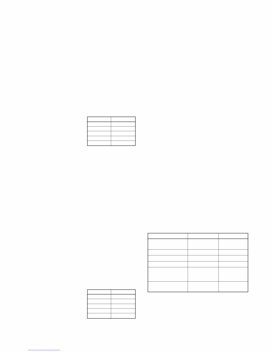
• AGC CIRCUIT
AGC line
RFGV
(RF gain control)
AGC
FAST
Q771
8 V
D771 C771
C772
2nd IF
signal
C775 R778 Q773
C774 R777 Q772
C773 R776
R775
D772 R772
R773
R774
Amp.
AGC
amp.
Q776, Q777
IC811b
“SML”
AGC det.
S-meter signal
Downloaded from www.Manualslib.com manuals search engine
3 - 4
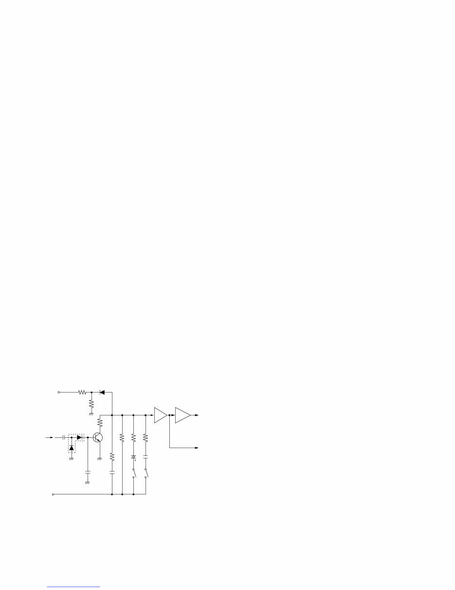
3-1-14 AF SELECTOR SWITCH (MAIN BOARD)
The AF signals from one of the detector circuits are applied
to the AF selector switch (IC861). IC861 consists of dual 4-
channel analog switches which are selected with a mode
signal and the squelch control signal.
3-1-15 AF AMPLIFIER CIRCUIT (PLL UNIT)
The AF amplifier amplifies the demodulated signal to a suit-
able driving level for the speaker.
The AF signals from the AF selector switch (MAIN board;
IC861) are applied to the PLL unit via the “AFI” signal line.
The CW side tone/beep tone and optional synthesized voice
are also applied to the PLL unit via the “AFBP” signal line.
The AF signals from the MAIN board are applied to the VCA
(Voltage Controlled Amplifier) circuit (IC201). The AF gain
setting from the main CPU is converted to DC voltage at the
D/A converter (MAIN board IC2201) and applied to the VCA
control terminal (IC201, pin 8) via the “AFGC” signal line.
The output AF signal from IC201 (pin 9) is power-amplified
at IC231 to drive the speaker.
3-2 TRANSMITTER CIRCUITS
3-2-1 MICROPHONE AMPLIFIER CIRCUIT
(MAIN BOARD)
The microphone amplifier circuit amplifies microphone input
signals and outputs the amplified signals to the balanced
modulator or FM modulation circuit.
Audio signals from the front or rear panel [MIC] connector
enter the microphone amplifier IC (IC931, pin 22) and are
then amplified at the microphone amplifier or speech com-
pressor section. Compression level is adjusted with the
[COMP GAIN] control (R945).
The amplified or compressed signals are applied to the VCA
section of IC931. The microphone gain setting from the D/A
converter (IC2201, pin 2) is applied to the VCA control ter-
minal (IC931, pin 10). The resulting signals from pin 9 are
then applied to the buffer amplifier (Q961) via the analog
switch (IC1141). External modulation input from the [ACC]
socket (pin 11) is also applied to Q961.
While in SSB mode, the amplified signals from the buffer
amplifier (Q961) are passed through the AF selector switch
(IC971) and are then applied to the balanced modulator
(IC1041).
While in AM/FM mode, the amplified signals from the buffer
amplifier (Q961) are applied to the limiter amplifier (IC981a)
and splatter filter (IC981b). The signals are then applied to
the AF selector switch (IC971) in AM mode or to the varac-
tor diode (D1012) in FM mode.
3-2-2 VOX CIRCUIT (MAIN BOARD)
The VOX (Voice-Operated-Transmission) circuit sets trans-
mitting conditions according to voice input.
When the VOX function is activated, the microphone signals
from IC931 (pin 19) are applied to the VOX comparator sec-
tion in the main CPU (IC2001, pin 32) via the VOXL line.
A portion of the power amplified AF signals from the AF
power amplifier (PLL unit; IC231) are amplified at the buffer
amplifier (IC931, pins 14, 15) and applied to the anti-VOX
comparator section in the main CPU (IC2001, pin 33) via the
AVXL line.
Then the main CPU compares these and controls the trans-
mitter circuit.
3-2-3 BALANCED MODULATOR (MAIN BOARD)
The balanced modulator converts the AF signals from the
microphone amplifier to a 9 MHz IF signal with a BFO (Beat
Frequency Oscillator) signal.
Microphone signals from the AF selector switch (IC971) are
applied to the balanced modulator (IC1041, pin 1). The BFO
signal from the PLL unit is applied to IC1041 (pin 10) as a
carrier signal.
IC1041 is a double balanced mixer IC and outputs a double
side band (DSB) signal with –40 dB of carrier suppression.
R1045 adjusts the balanced level of IC1041 for maximum
carrier suppression. The resulting signal passes through a 9
MHz IF filter (FI671 in SSB/CW/RTTY modes) to suppress
unwanted side-band signals.
In AM mode, R1042 is connected to upset the balance of
IC1041 via Q1041 for leaking the BFO signal as a carrier
signal. The CW keying/RTTY TX signal is applied to IC1041
pin 1.
• AF selector switch
11
13
INH
15
12
9, 10
14
X3
X2
X0
X
X1
SSB/CW/
RTTY
IC861
FM
WFM
AM
6
AFS1, AFS2
SQL
AFI signal
to PLL unit
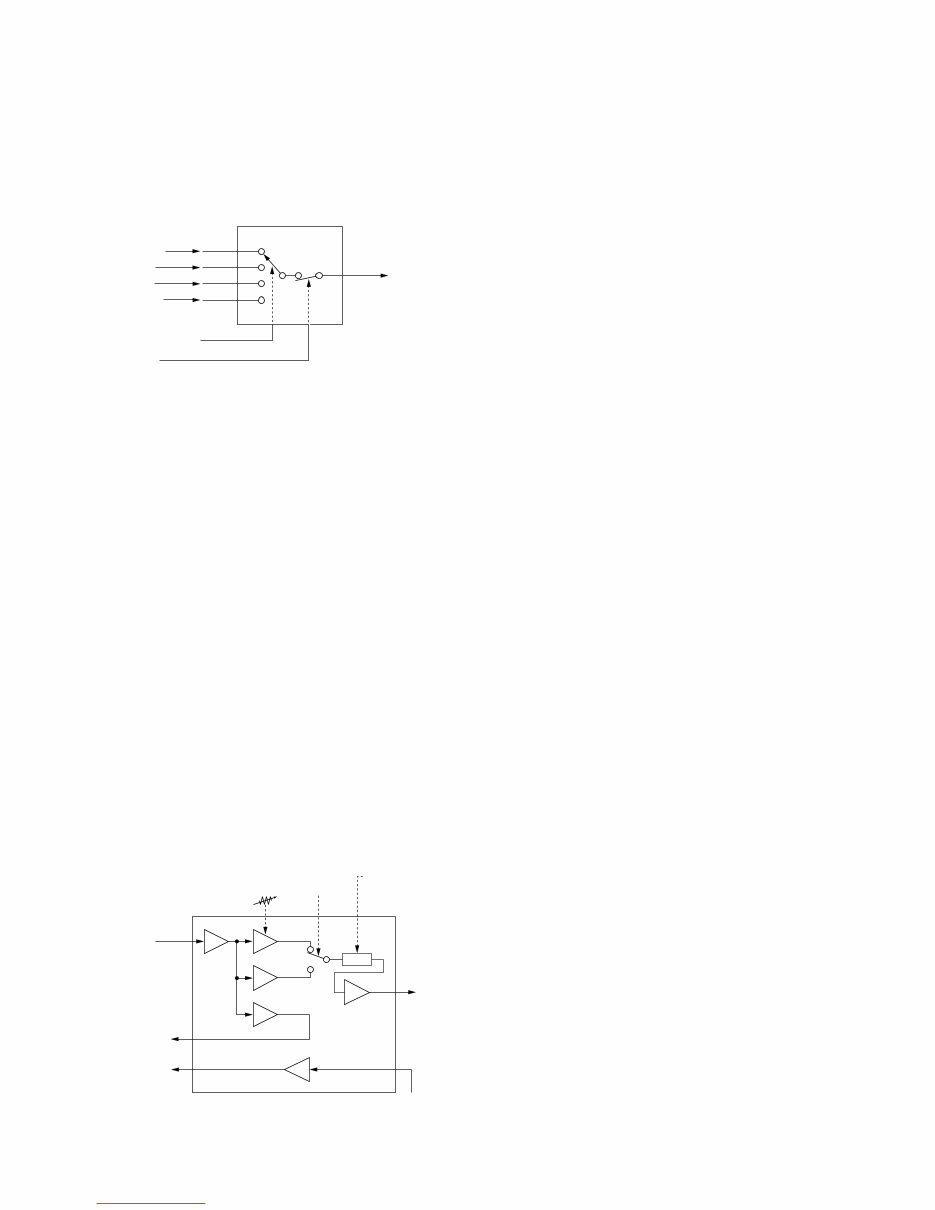
• Microphone amplifier
11 2, 3 10
19
22
9
14 15
MIC
signal
IC931
[COMP GAIN]
(R945)
MIGV from D/A
convertor (IC35)
VOXL
to CPU
AVOXL
to CPU
AFO signal
Amp.
COMP
Buffer
Buffer
Buffer
COMS
from CPU
AMOD
to IC1141
VCA
Buffer
Downloaded from www.Manualslib.com manuals search engine

3 - 5
3-2-4 FM MODULATION CIRCUIT (MAIN BOARD)
The microphone signals from Q961 are applied to the limiter
amplifier (IC981a) and the splatter filter (IC981b). The 1750
Hz European tone signal from the main CPU (IC2001 pin
40) is also applied to IC981a pin 2 for European repeaters.
The sub-audible tone signal (67.0–254.1 Hz) from the main
CPU (IC2001 pin 37) is also applied to IC981b pin 5 for
repeater use.
The resulting signals are applied to the VCO circuit (Q1011,
D1012) via R1002 to change the reactance of the varactor
diode (D1012) for FM modulation. The modulated signal is
amplified at the buffer amplifier (Q1013) and bypasses the 9
MHz IF filter.
3-2-5 TRANSMITTER IF CIRCUIT (MAIN BOARD)
The 9 MHz IF signal from the modulation circuit passes
through the 9 MHz IF filter (FI671 in SSB/CW/RTTY modes;
FI681 in AM/FM-N modes; through in FM mode). The signal
is amplified at IC571, and then passes through the total gain
adjustment volume (R579), and the crystal filter (FI561). The
signal is then applied to the 2nd mixer (D551).
The signal is mixed with the 2nd LO signal (60 MHz) and
converted to a 69 MHz IF signal at the 2nd mixer (D551).
The 69 MHz IF signal passes through a bandpass filter, IF
amplifier (IC521) and 69 MHz IF filter (FI511), and is then
converted to the displayed frequency at the 1st mixer (D271)
with the 1st LO signal. The mixers (D271, D551) and IF
amplifiers (IC521, IC571) are used commonly for both
receiving and transmitting.
The ALC voltage is supplied to the transmit/receive switch-
ing circuit (D521/D522 and D572/D573). D521/D522 and
D572/D573 function as PIN attenuators for ALC operation.
3-2-6 RF CIRCUIT
(PA UNIT, MAIN AND HPF BOARD)
The RF circuit amplifies the displayed frequency signal to
obtain 100 W of RF output power for HF/50 MHz bands and
50 W for the 144 MHz band, 20 W for the 440 MHz band.
The HF/50 MHz RF signals from the 1st mixer (D271) via the
low-pass filter enter the HPF board and then pass through
one of 8 high-pass filters (Refer to 3-1 for used RF high-pass
filter). The 50 MHz RF signals pass through a low-pass filter
additionally. The filtered signals return to the MAIN board,
are amplified at the YGR amplifier (IC231), and are then
applied to the PA unit.
The 144 MHz RF signals from the 1st mixer (D271) via the
low-pass filter (L251–253, C253–259) bypass the filters and
pass through the bandpass filter (L182–L184, L195, L196,
C181–C186, C195–C197) in the MAIN board. The signals
are amplified at the RF amplifier (IC221) and YGR amplifer
(IC231) and are then applied to the PA unit.
The 440 MHz RF signals from the 1st mixer (D271) via the
low-pass filter (L251–253, C253–259) are amplified at RF
amplifier (IC222) and passed through the bandpass filter
(FI371–FI373) in the MAIN board. The filtered signal is
amplified at the YGR amplifer (IC231) and is applied to the
PA unit.
The signals from IC231 enter the PA unit and is amplified at
the drive amplifiers (Q101, Q121) in sequence. The ampli-
fied signals are applied to the band switch (RL1).
The HF/50 MHz RF signals from the band switch (RL1) are
amplified at the drive (DRIVER board; Q161) and power
(Q171, Q172) amplifiers to obtain a stable 100 W of RF out-
put power. The power-amplified signals are then applied to
the [ANT1] connector via one of the 7 low-pass filters in the
FILTER board.
For the 144/440 MHz RF signals from the band switch
(RL1), 50 W for 144 MHz band or 20 W for 440 MHz band
of RF output power is obtained at the drive (DRIVER board;
Q211) and power amplifier (Q231). The power-amplified sig-
nals are applied to the [ANT2] connector via the antenna
switching circuit and low-pass (144 MHz band) or high pass
(440 MHz band) filters.
3-2-7 ALC CIRCUIT (MAIN BOARD)
The ALC (Automatic Level Control) circuit reduces the gain
of IF amplifiers in order for the transceiver to output a con-
stant RF power set by the RF power setting even when the
supplied voltage shifts, etc.
The HF/50 MHz RF power signal level is detected at the
power detector (FILTER board; D9), buffer-amplified at IC1b
and applied to the MAIN board as the “HFOR” voltage.
The 144 MHz and 440 MHz RF power signals are detected
at the power detectors (PA unit; D262, D263) and (PA unit;
D312, D313) respectively. The detected signals are applied
to the MAIN board as the “VFOR” or “UFOR” voltages.
• TRANSMITTER CONSTRUCTION
1st LO 60.0 MHz
BFO
FM tone
D551
IC231
[ANT1]
HF+50 MHz
[ANT2]
144/440 MHz
144 MHz
440 MHz
Q101
Q121
Q171
Q172
Q231
Q1011 D231
IC1041
IC931
Crystal
filter
FI1
FI671, FI681,
or optional filter
MIC
except FM
9.0115 MHz
Crystal
filter
BPF
BPF
LPF
LPF
HPF
BPF
HPF
HPF
PA UNIT
HPF
BOARD
FILTER
BOARD
MAIN BOARD
Amp. Amp. Amp.
Amp.
Q161
Amp.
Amp.
Q211
Amp.
IDC
FM, AM
AM
FM
FM only
50 MHz
144 MHz
SSB
•
•
•
BPF
440 MHz
Downloaded from www.Manualslib.com manuals search engine
You're Reading a Preview
What's Included?
Fast Download Speeds
Online & Offline Access
Access PDF Contents & Bookmarks
Full Search Facility
Print one or all pages of your manual
$41.99
ICOM IC-706MKIIG Service Repair Manual
Viewed 16 Times Today

What's Included?
Fast Download Speeds
Online & Offline Access
Access PDF Contents & Bookmarks
Full Search Facility
Print one or all pages of your manual
$41.99

Secure transaction
What's Included?
Fast Download Speeds
Online & Offline Access
Access PDF Contents & Bookmarks
Full Search Facility
Print one or all pages of your manual
Description
The Factory Service Manual is an essential resource for car repair, providing a comprehensive range of technical information. It includes schematic diagrams, block diagrams, adjustment procedures, board layouts, and more.
SUMMARY OF CONTENTS:
- Specifications
- Inside Views
- Circuit Description
- Adjustment Procedures
- Parts List
- Mechanical Parts
- Dis-assembly
- Semi-Conductor Information
- Board Layouts
- Block Diagram
- Voltage Diagram
ABOUT THIS MANUAL
- PAGES: 85
- LANGUAGE: English
- DOCUMENT ID: A-5564HI-S
- PUBLICATION YEAR: 1999
- Has bookmarks for easy navigation: Yes
- Can be printed: Yes
- Can be edited: Yes (No password, No security)
- Windows compatible / Mac compatible
OUR GUARANTEE
- Every manual has been reviewed by humans for quality, correct number of pages, and bookmarks.
- The illustration above is a small preview from an actual screenshot of this manual.
Icom IC-706MKIIG Service Manual


