

Service Manual CASIO CTK-511 ELECTRONIC KEYBOARD
What's Included?
Fast Download Speeds
Online & Offline Access
Access PDF Contents & Bookmarks
Full Search Facility
Print one or all pages of your manual
ELECTRONIC KEYBOARD
CTK-511
CTK-511

CONTENTS
Specifications ................................................................................................................................... 1
Block Diagram .................................................................................................................................. 2
Circuit Description ............................................................................................................................ 3
Adjustment ....................................................................................................................................... 7
Major Waveforms ............................................................................................................................. 8
Printed Circuit Boards ...................................................................................................................... 9
Schematic Diagrams ...................................................................................................................... 10
Exploded View ............................................................................................................................... 15
Parts List ........................................................................................................................................ 16

— 1 —
SPECIFICATIONS
GENERAL
Keyboard: 61 standard-size keys, 5 octaves
Tones: 100
Polyphony: 12 notes maximum (6 for certain tones)
Auto accompaniment
Rhythm patterns: 100
Tempo: Variable (236 steps, = 20 to 255)
Chords: 2 fingering methods (CASIO CHORD, FINGERED)
Rhythm controller: START/STOP, SYNCHRO/FILL-IN
Accomp volume: 0 to 9 (10 steps)
Song bank
Tunes: 100
Controllers: PLAY/PAUSE, STOP, REW, FF, LEFT ON/OFF (ACCOMP), RIGHT ON/
OFF (MELODY)
Display
Name display: TONE, RHYTHM, SONG BANK name/number, keyboard settings name/value
Tempo: Tempo value, metronome, synchro standby, beat indicator
Chord: Chord name, Chord form
Fingering: Fingering indicators, parts, pedal
Song bank status: PLAY, PAUSE, REW, FF
Staff: 5 octaves with sharp and flat indications
Keyboard: 5 octaves
MIDI: 5 multi-timbre receive
Other functions
Transpose: 12 steps (–6 semitones to +5 semitones)
Tuning: Variable (A4 = approximately 440 Hz ± 50 cents)
Volume: 0 to 9 (10 steps)
Terminals
MIDI terminals: IN, OUT
Sustain terminal: Standard jack
Phones/Output terminal: Stereo standard jack
Output Impedance: 78 Ω
Output Voltage: 4 V (RMS) MAX
Power supply terminal: 9 V DC
Power supply Dual power supply system
Batteries: 6 D-size batteries
Battery life: Approximately 8 hours on manganese batteries
AC adaptor: AD-5
Auto power off: Turns power off approximately six minutes after last key operation. Enabled
under battery power only, can be disabled manually.
Speaker output: 2.0 W + 2.0 W
Power consumption: 9 V --- 7.7 W
Dimensions (HWD): 961 × 381 × 139 mm (37-7/8 × 15-1/16 × 5-1/2 inches)
Weight: Approximately 5.4 kg (11.91 lbs) (without batteries)
ELECTRICAL
Current drain with 9 V DC:
No sound output 250 mA ± 20%
Maximum volume 830 mA ± 20%
with 12 keys C1 to B1 pressed in Synth-Lead 1
Volume: Maximum
Phone output level (Vrms with 8 Ω load each channel):
with key G2 pressed in Synth-Lead 1 78 mV ± 20%
Speaker output level (Vrms with 4 Ω load each channel):
with key G1 pressed in Synth-Lead 1 1250 mV ± 20%
Output level (Vrms with 47 KΩ load each channel):
with key B1 pressed in Synth-Lead 1 1050 mV ± 20%
Minimum operating voltage: 6.0 V
— 2 —
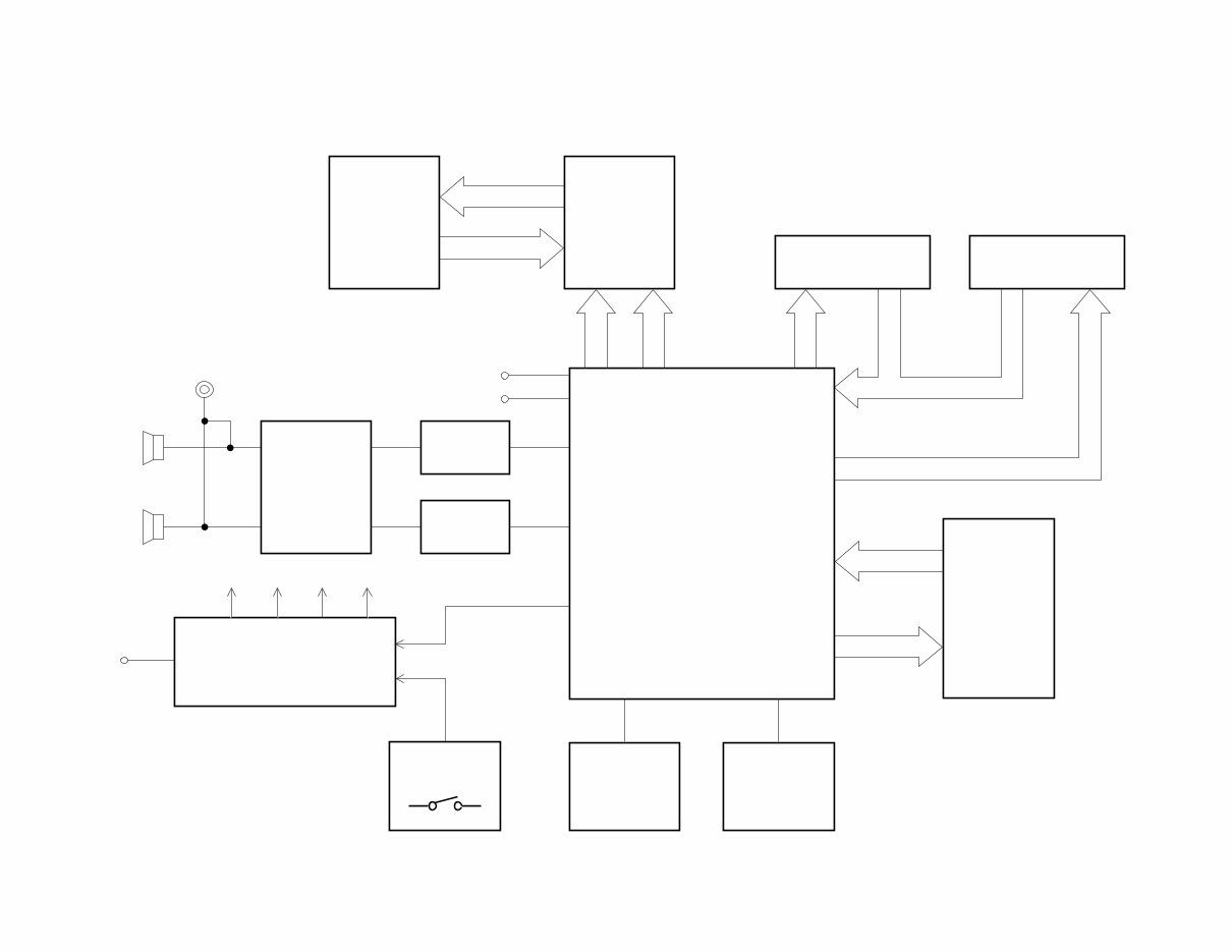
BLOCK DIAGRAM
CPU
MSM 6755B-17
LSI2
Keyboard
Buttons
LCD
LCD Driver
SED1278F2A
LSI3
Reset IC
RN5VD40A
IC1
Oscillator
X1, Q1
Power Supply Circuit
Q201 ~ Q203, Q207, Q208, D205
Power Amp.
TA8248K
IC201
Filter (L)
Q206
Filter (R)
Q205
Phone/Output
VC VCC DVDD AVDD
APO
DC + 9V IN
DB4 ~ DB7
MIDI IN
MIDI OUT
COM1 ~ COM16
SEG1 ~ SEG40
RS
R/W
E
KO8 ~
KO12
KI0 ~ KI6
KO0 ~ KO7
MD0 ~ MD7
MA0 ~ MA18
ROM(2M-bit)
LC372100PM-
G48
LSI1
Power Switch
— 3 —
CIRCUIT DESCRIPTION
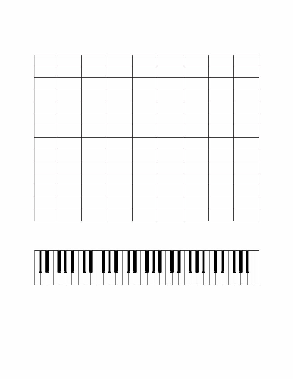
KEY MATRIX
NOMENCLATURE OF KEYS
KI0 KI1 KI2 KI3 KI4 KI5 KI6 KI7
KO0 C2 G#2 E3 C4 G#4 E5 C6 G#6
KO1 C#2 A2 F3 C#4 A4 F5 C#6 A6
KO2 D2 A#2 F#3 D4 A#4 F#5 D6 A#6
KO3 D#2 B2 G3 D#4 B4 G5 D#6 B6
KO4 E2 C3 G#3 E4 C5 G#5 E6 C7
KO5 F2 C#3 A3 F4 C#5 A5 F6
KO6 F#2 D3 A#3 F#4 D5 A#5 F#6
KO7 G2 D#3 B3 G4 D#5 B5 G6
KO8 — + 0
KO9 3 2 1
KO10 6 5 4 Rhythm Tone
KO11 9 8 7 Fingered Normal Off
KO12 FF Right Stop Left REW
Tempo
Down
Tempo
Up
Start/
Stop
Synchro/
Fill-In
Chord
Book
Accomp
Volume
Transpose/
Tune/MIDI
Song
Bank
CASIO
Chord
Play/
Pause
Volume
Down
Volume
Up
F#3 G#3 A#3 C#4 D#4 F#4 G#4 A#4 C#5 D#5 F#5 G#5 A#5
F3 G3 A3 B3 C4 D4 E4 F4 G4 A4 B4 C5 D5 E5 F5 G5 A5 B5 C6
D#3
C2 D2 E2 F2 G2 A2 B2 C3 D3 E3 B6 A6 G6 F6 E6 D6 C7
C#3 A#2 G#2 F#2 D#2 C#2 A#6 G#6 F#6 D#6 C#6
— 4 —
CPU (LSI2: MSM6755B-17)
The CPU reads sound data from the ROM in accordance with the pressed key and the selected tone; the CPU
can read rhythm data simultaneously when a rhythm pattern is selected. Then it provides the left and the right
channels’ waveforms separately, by converting the data into the waveforms with two built-in DACs. The CPU
also controls key and button input. The following table shows the pin functions of LSI2.
Pin No. Terminal In/Out Function
1 MA14 Out Address bus
2, 3 NCO — Not used
4 ~ 19 MA0 ~ MA13 Out Address bus
13 MRDB Out Read enable signal
17 MCSB — Not used
20 ~ 27 MD0 ~ MD7 In/Out Data bus
28, 29 NC1, NC2 — Not used
30 DGND In Ground (0 V) source
31 DVCC In +5 V source
32, 33 XTLO, XTLI In/Out 20 MHz clock input/output
34 NC3 — Not used
35 RSTB In Reset signal input
36 P24/RXD In MIDI signal input
37 P25/TXD Out MIDI signal output
38 NMI In Power ON signal input. Connected to +5 V.
39 APO Out APO (Auto Power Off) signal output
40 NC4 — Not used
41 REFH Out Terminal for the internal DAC
42, 43 NC5, NC6 — Not used
44 DAOR Out Right channel sound waveform output
45 NC7 — Not used
46 AVdac In +5 V source for the internal DAC
47 DAOL Out Left channel sound waveform output
48 REFL Out Terminal for the internal DAC and ADC
49 AGdac In Ground source for internal DAC
50 AGadc In Ground source for internal ADC
51 ANI In APO cancellation signal
52 AVadc In +5 V source for the internal ADC
53 NC8 — Not used
54 MOD0 In Mode selection terminal. Connected to +5 V.
55, 56 MOD1, MOD2 In Mode selection terminal. Connected to ground.
57 P40 In Pedal signal input
58 ~ 64 KI0/P30 ~ KI7/P36 In Terminals for key/button input signal
65 KI7/P37 — Not used
66 ~ 73 KO0/P50 ~ KO7/P57 Out Terminals for key scan signal
— 5 —
LCD DRIVER (LSI3: SED1278F2A)
The LCD driver can drive a dot matrix LCD having 40 segment and 16 common lines. The LSI contains 240
graphic symbols in the built-in character generator ROM, and stores 80 characters in the built-in display data
RAM. In accordance with command from the CPU, the LSI is capable of displaying up to 16 characters
simultaneously. The following table shows the pin functions of LSI3.
Pin No. Terminal In/Out Function
74 ~ 77 DB4 ~ DB7 Out Data bus for the LCD driver
78 NC9 — Not used
79 LVCC In +5 V source
80 ~ 84 KO8 ~ KO12 Out Terminals for button scan signal
85 ~ 87 P65 ~ P67 — Not used
88 RS Out Control signal for the LCD driver
89 R/W Out Read/Write signal for the LCD driver
90 E Out Chip enable signal for the LCD driver
91 ~ 95 P73 ~ P77 — Not used
96 LGND In Ground source
97, 100 MA18, MA15 Out Address bus
Pin No. Terminal In/Out Function
1 ~ 22,
63 ~ 80
23 VSS — GND (0 V) source
Terminals for the built-in clock pulse generator. The external
resistor connected determines the oscillation frequency.
LCD drive voltage input.
26 ~ 30 V1 ~ V5 In Those voltages are used for generating the stepped pulse of
the LCD drive signals.
31, 32 LP, XCLS — Not used
33 VDD In DVDD (+5 V) source
34, 35 FR, DO — Not used
Data/command determination terminal.
High: data, Low: command
37 R/W In Read/Write terminal. High: read, Low: write
Chip enable signal.
38 E In High: enable, the writing is done at fall edge.
Low: disenable
39 ~ 42 DB0 ~ DB3 — Not used. Connected to GND (0 V)
43 ~ 46 DB4 ~ DB7 In/Out Data bus
47 ~ 62 COM1 ~ COM16 Out Common signal/output
SEG1 ~ SEG40 Out Segment signal output
24, 25 OSC1, OSC2 In/Out
36 RS In
— 6 —
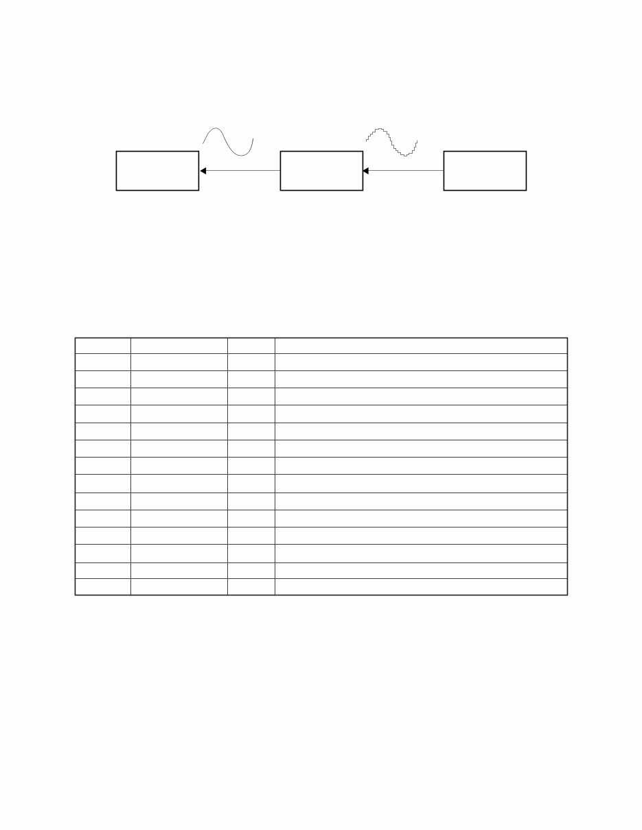
FILTER BLOCK
Since the sound signals from the CPU is stepped waveforms, the filter block is added to smooth the waveforms.
POWER AMPLIFIER (IC201: TA8248K)
The power amplifier is a two-channel amplifier with standby switch.
The following table shows the pin function of IC201.
Pin No. Terminal In/Out Function
1 NC — Not used
2 B.S.2 — Terminal for a bootstrap capacitor
3 OUT2 Out Channel 2 output
4 VCC In +9 V source
5 OUT1 Out Channel 1 output
6 B.S.1 — Terminal for a bootstrap capacitor
7 Power GND In Ground (0 V) source
8 Stand by In Power control signal input. 0 V: Off, +9 V: On
9 DC — Terminal for a decoupling capacitor
10 NF1 In Negative feedback input
11 IN1 In Channel 1 input
12 IN2 In Channel 2 input
13 NF2 In Negative feedback input
14, 15 Pre GND In Ground (0 V) source
Amp.
TA8248K
Filter
Block
CPU
MSM6755B-17
— 7 —
Output
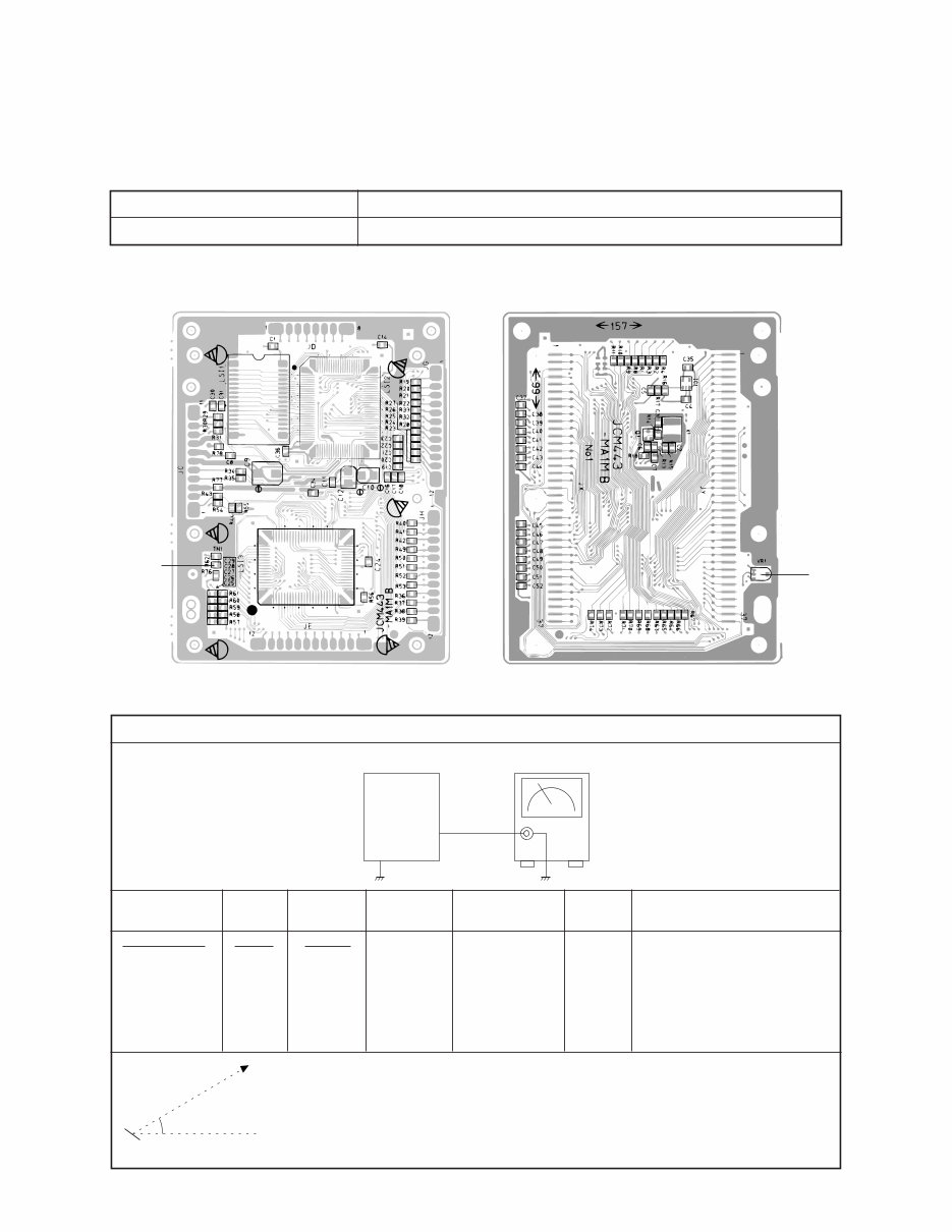
Set Voltmeter
R62
3) Equipment connection/Procedure
Vop voltage setting
Input
Connection
Input
Point
Input
Signal
Adjust
Output
Connection
Output
Point
Adjust for
VR1 Voltmeter R62 Adjust for 4.40 ~ 4.46 V read-
ing on voltmeter under the
temparature 20 ~ 25 °C.
Make fine adjustment accord-
ing to the following instruc-
tion.
Watching the LCD at a 37° angle to the horizontal, adjust Vop
voltage so that unenergized segments are seen dimly.
ADJUSTMENT
MAIN PCB
1) Items to be adjusted:
2) Adjustment and Test Point Locations
(TOP VIEW)
Item Measuring Instrument
Vop voltage setting Voltmeter
37°
LCD
Eye
(BOTTOM VIEW)
Test point
VR1

— 8 —
MAJOR WAVEFORMS
1 Clock pulse
MSM6755B-17 pin 32
1
2 Power source DVDD
JC connector pin 8
3 APO signal
JC connector pin 2
2
3
4 Sound waveform (R-ch) Tone: Whistle (59)
JC connector pin 5 Key: A4
5 Sound waveform (L-ch) Volume: Max.
JC connector pin 4
4
5
6 Button scan signal KO0
MSM6755B-17 pin 66
7 Button scan signal KO1
MSM6755B-17 pin 67
6
7
8 LCD common signal COM6
SED1278F2A pin 52
9 LCD common signal COM7
SED1278F2A pin 53
8
9
You're Reading a Preview
What's Included?
Fast Download Speeds
Online & Offline Access
Access PDF Contents & Bookmarks
Full Search Facility
Print one or all pages of your manual
$31.99
Viewed 16 Times Today


Secure transaction
What's Included?
Fast Download Speeds
Online & Offline Access
Access PDF Contents & Bookmarks
Full Search Facility
Print one or all pages of your manual
$31.99
This is a comprehensive Workshop Service/Repair Manual for the CASIO CTK-511 ELECTRONIC KEYBOARD. It functions on all PC-based Windows operating systems and Mac, providing technical repair information for rebuilding or maintaining your electronic keyboard.
It includes:
- Specifications
- Block Diagram
- Circuit Description
- Adjustment
- Major Waveforms
- Printed Circuit Boards
- Schematic Diagrams
- Exploded View
- Parts List
- And more...
Total Pages: 21
Format: PDF
Language: English
Compatibility: Win/Mac
This service manual is essential for flawless repairs and maintenance of the CASIO CTK-511 ELECTRONIC KEYBOARD, with included pictures and diagrams for better understanding. All pages are printable, allowing you to print the entire guide or specific sections.
Benefits:
- Instant access
- No shipping cost
- No need to wait for a CD-ROM to arrive in the mail
Get your own copy now!


