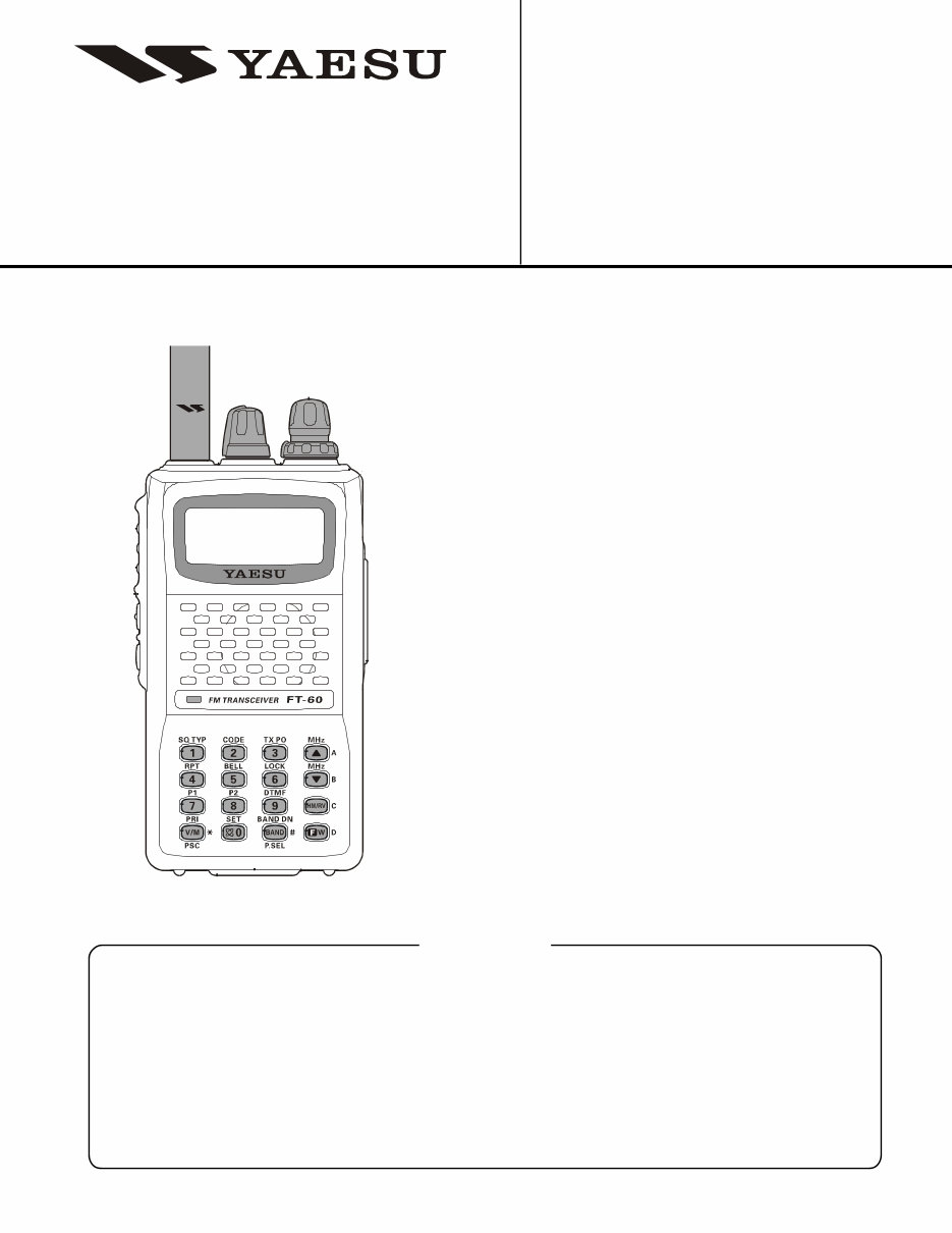
2 Specifications General Frequency Ranges: RX 108 - 137 MHz (Air Band), (Cellular Blocked) 137 - 520 MHz (AM/FM), 700 - 999.990 MHz (FM) TX 144-148 MHz, 430-450 MHz Channel Steps: 5/10/12.5/15/20/25/50/100 kHz Frequency Stability: ±5 ppm @ 14 °F to 140 °F (–10 °C to +60 °C) Repeater Shift: ±600 kHz (144 MHz), ±1.6/5.0/7.6 MHz (430 MHz) Emission Type: F2 (F2D), F3 (F3E) Antenna Impedance: 50 W Supply Voltage: Nominal: 7.2 V DC, Negative Ground (Negative Ground) Operating: 6.0 ~ 16.0 V DC (EXT DC Jack) 11.0 ~ 16.0 V DC (EXT DC Jack with Charging) Current Consumption: 125 mA (Receive) (Approx. @7.2 V) 45 mA (144 MHz, Standby, Saver Off) 47 mA (430 MHz, Standby, Saver Off) 19 mA (Standby, Saver On) 0.8 mA (Auto Power Off) 1.5 A (5 W TX, 144 MHz) 1.6 A (5 W TX, 430 MHz) Operating Temperature: –4 °F to 140 °F (–20 °C to +60 °C) Case Size: 2.3” (W) x 4.3” (H) x 1.2” (D) (58 x 109 x 30 mm) (W/O knob, antenna, and belt clip) Weight: 13.05 Oz (370 g) with FNB-83, and antenna Transmitter RF Power Output: 5.0 W (High) / 2.0 W (Middle) / 0.5 W (Low) (Approx.) Modulation Type: Variable Reactance F2 (F2D), F3 (F3E) Maximum Deviation: ±5.0 kHz (F2D, F3E) Spurious Emission: At least 60 dB down (@ High and Middle power) At least 40 dB down (@ Low power) Microphone Impedance: 2 kW Receiver Circuit Type: Double-Conversion Superheterodyne Intermediate Frequencies: 1st: 47.25 MHz, 2nd: 450 kHz Sensitivity : 0.8 µV TYP for 10 dB SN (108-137 MHz, AM) (Cellular Blocked) 0.2 µV for 12 dB SINAD (137-140 MHz, FM) 0.16 µV for 12 dB SINAD (140-150 MHz, FM) 0.2 µV for 12 dB SINAD (150-174 MHz, FM) 0.3 µV TYP for 12 dB SINAD (174-300 MHz, FM) 0.8 µV for 10 dB SN (300-336 MHz, AM) 0.25 µV for 12 dB SINAD (336-420 MHz, FM) 0.2 µV for 12 dB SINAD (400-470 MHz, FM) 0.25 µV for 12 dB SINAD (470-520 MHz, FM) 0.5 µV TYP for 12 dB SINAD (800-900 MHz, FM) 0.8 µV TYP for 12 dB SINAD (800-999.990 MHz, FM) Selectivity: 12 kHz/35 kHz (–6 dB /–60 dB) AF Output: 400 mW @ 8 W for 10 % THD (@ 7.5 V) Specifications are subject to change without notice, and are guaranteed within the 144 and 430 MHz amateur bands only. Frequency ranges will vary according to transceiver version; check with your dealer.
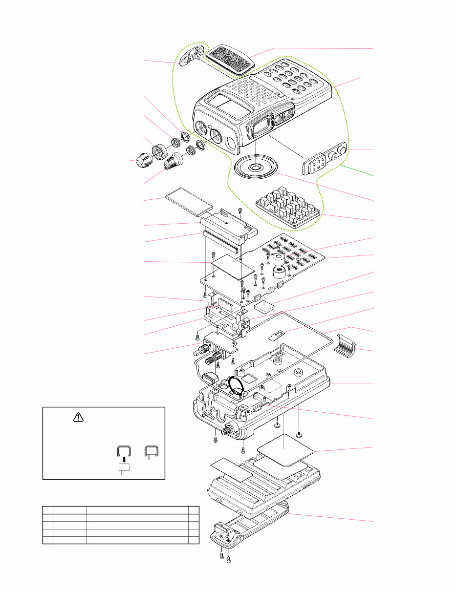
3 Exploded View & Miscellaneous Parts Screw List RA0321900 RUBBER CAP RA0611600 WINDOW RA0210600 RUBBER PACKING (x2 pcs) RA0209900 KNOB RA0209800 KNOB RA0209700 VOLUME KNOB G6090160 LCD RA0322000 RUBBER RA032090B LCD HOLDER RA0324700 INTER CONNECTOR RA0324800 REFLECTOR SHEET RA0211200 INTER CONNECTOR RA0107000 TERMINAL PLATE R (x2 pcs) VR-Unit RA0595200 HOLDER RA0322800 TERMINAL PLATE RA0110200 HOLDER RUBBER CP7970001 BELT CLIP ASSY RA0613500 RUBBER KNOB RA0599500 FRONT CASE ASSY (W/ MIC SHEET, PACKING PAD(YER), SP NET,LIGHT GUIDE, DOUBLE FACE(WINDOW)) RA021020A RUBBER PACKING RA0111400 RING NUT (x2 pcs) RA021080A (Lot. 5-) SPACER RA0210800 (Lot. 1-4) SPACER RA0318700 BLIND SHEET CP7969001 REAR CASE ASSY (W/ SMA CNNECTOR) M4090142B SPEAKER RA055770B (Lot. 31-) LATCH NAIL C RA0123500 (Lot. 1-30) LATCH NAIL B CAUTION The mic element must be desoldered and removed from the PCB on order to rein- stall its protective rubber cover. Therefore, be careful not to remove this cover unless mic ele- ment replacement is necessary. ➀ ➁ Non-designated parts are available only as part of a designated assembly. Qty. 14 2 2 2 VXSTD P/N U9900068 U9900063 U9900051 U02206007 No. ➀ ➁ ➂ ➃ Description TAPTITE SCREW M2X4NI#3 TAPTITE SCREW 2X3.3NI TAPTITE SCREW M2X4B#3 SEMS SCREW SM2.6X6B ➀ ➀ ➀ ➀ ➀ ➀ ➀ ➀ ➀ ➀ ➀ ➀ ➀ ➀ ➁ ➁ ➂ ➂ ➃ ➃ RA0616500 SPONGE RUBBER CP7968001 PANEL ASSY RA0618700 PAD (x2 pcs) MAIN-Unit
4 Exploded View & Miscellaneous Parts Note
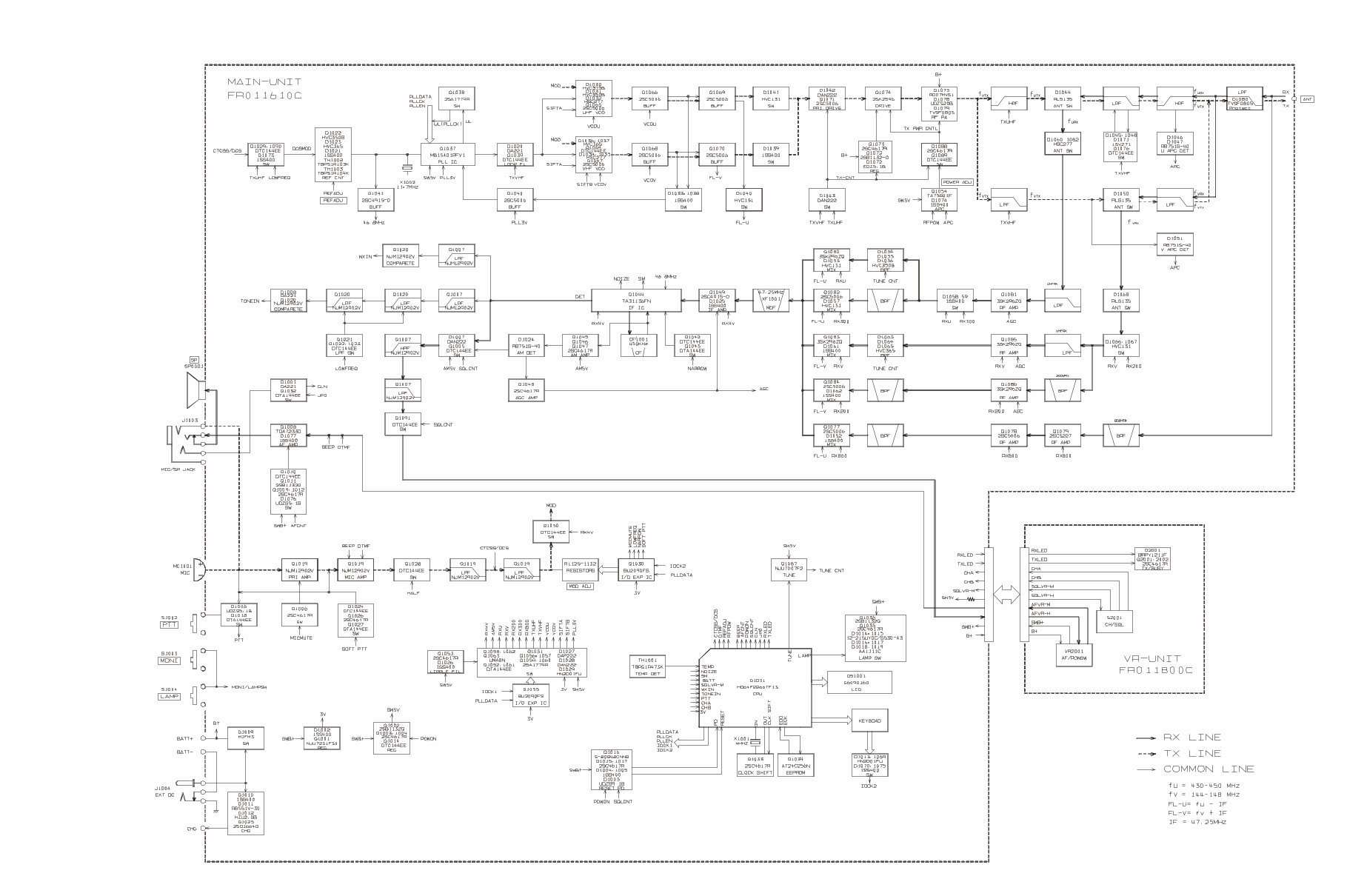
5 Block Diagram
6 Block Diagram Note
7 Circuit Description VHF Reception Incoming VHF signal is passed through the low-pass fil- ter network, antenna switching diode D1066 (HVC131) and D1068 (RLS135), and low-pass filter network to the RF amplifier Q1085 (3SK296ZQ). The amplified RF sig- nal is passed through band-pass filtered again by varac- tor-tuned resonators L1060, L1061 and L1062, and D1063, D1064, and D1065 (all HVC365), then applied to the 1st mixer Q1083 (3SK296ZQ) along with the first local signal from the PLL circuit. The first local signal is generated between 191.25 MHz and 195.25 MHz by the VHF VCO, which consists of Q1067 ( 2SC5006 ), switching diodes D1034, D1035 (both HSC277 ), and varactor diodes D1036, D1037 (both HVC365) according to the receiving frequency. UHF Reception Incoming UHF signal is passed through the low-pass fil- ter network, antenna switching diodes D1060 and D1082 (both HSC277), and Low-pass filter network to the RF am- plifier Q1081 (3SK296ZQ). The amplified RF signal is passed through band-pass filtered again by varactor-tuned resonators L1049, L1050 and L1051, and D1054, D1055, and D1056 (all HVC350B), then applied to the 1st mixer Q1080 (3SK296ZQ) along with the first local signal from the PLL circuit. The first local signal is generated between 382.75 MHz and 402.75 MHz by the UHF VCO, which consists of Q1065 (2SC5006) and varactor diodes D1030 (HVC375B), D1031 (HVC350B) and switching diode D1032 (HSC277) accord- ing to the receiving frequency. IF and Audio Circuits The 47.25 MHz first IF signal is applied to the monolithic crystal filters XF1001 which strip away unwanted mixer products, and the IF signal is applied to the first IF ampli- fier Q1049 (2SC4915). The amplified first IF signal is then delivered to the FM IF subsystem IC Q1044 (TA31136FN), which contains the second mixer, limiter amplifier, noise amplifier, and FM detector. The second local signal is generated by 46.8 MHz crystal X1002 and Q1041 (2SC4915), produces the 450 kHz sec- ond IF signal when mixed with first IF signal within Q1044 (TA31136FN). The 450 kHz second IF signal is applied to the ceramic filter CF1001 which strip away unwanted mixer products to the ceramic discriminator CD1001 which removes any amplitude variations in the 450 kHz IF signal before de- tection of speech. The detected audio passes through the de-emphasis net- work, low-pass filter consisting of Q1007 (NJM12902V) and associated circuitry, and high-pass filter consisting of Q1007 (NJM12902V) and associated circuitry. The filtered audio signal is applied to the audio volume, then passes through the AF ampplifire Q1008 (TDA7233D) and MIC/ SP jack to the internal speaker or an external speaker. Squelch Control When no carrier received, noise at the output of the de- tector stage in Q1044 (TA31136FN) is amplified and band- pass filtered by the noise amp section of Q1044 (TA31136FN). The resulting DC voltage is applied to pin 47 of main CPU Q1031 (HD64F2266), which compares the squelch threshold level to that which set by the SQL knob. While no carrier is received, pin 35 of Q1031 (HD64F2266) remains “low,“ squelch gate Q1005 and Q1091 (both DTC144EE) to turns off to disable any demodulated au- dio pass. Transmit Signal Path The speech signal from the microphone to AF amplified Q1019 (NJM12902V). The amplified speech signal passes through low-pass filter network Q1019 (NJM12902V) to deviation controlled by Q1030 (BU2090FS). VHF Transmit Signal Path The adjusted speech signal is delivered to VHF VCO Q1067 (2SC5006) which frequency modulates the trans- mitting VCO made up of D1037 (HVC365). The modulated transmit signal passes through buffer amplifier Q1068 and Q1070 (both 2SC5006). The filtered transmit signal applied to the Pre-Drive am- plifier Q1071 ( 2SC5006) and Drive amplifier Q1074 (2SK2596), then finally amplified by Power amplifier Q1075 (RD07MVS1) up to 5 Watts. This two stages pow- er amplifier's gain is controlled by the APC circuit. The 5 Watts RF signal passes through low-pass filter net- work, antenna switch D1050 (RLS135), and another low- pass filter network, and then deliver to the ANT jack. UHF Transmit Signal Path The adjusted speech signal is delivered to UHF VCO Q1065 (2SC5006) which frequency modulates the trans- mitting VCO made up of D1030 (HVC375). The modulated transmit signal passes through buffer amplifier Q1066 and Q1069 (both 2SC5006). The filtered transmit signal applied to the Pre-Drive am- plifier Q1071 ( 2SC5006) and Drive amplifier Q1074 (2SK2596), then finally amplified by Power amplifier Q1075 (RD07MVS1) up to 5 Watts. This two stages pow- er amplifier's gain is controlled by the APC circuit.
8 Circuit Description The 5 Watts RF signal passes through high-pass filter and high-pass filter network, antenna switch D1044 (RLS135), and another low-pass filter network, and then deliver to the ANT jack. TX APC Circuit A portion of the Power amplifier output is rectified by D1051 (UHF: D1046 and D1047) (all RB751S), then de- livered to APC Q1054 (TA75S01F), as a DC voltage which is proportional to the output level of the power amplifier. The APC Q1054 (TA75S01F) is compared the rectified DC voltage from the power amplifier and the reference volt- age from the main CPU Q1031 (HD64F2266), to produce a control voltage, which regulates supply voltage to the Drive amplifier Q1074 (2SK2596) and Power amplifier Q1075 (RD07MVS1), so as to maintain stable output power under varying antenna loading condition. PLL A portion of the output from the VCO Q1065 (UHF: 2SC5006) and Q1067 (VHF: 2SC5006), passes through buffer amplifier Q1066 (UHF), Q1068 (VHF), and Q1040 (all 2SC5006) programmable divider section of the PLL IC Q1037 (MB15A01PFV1), which divided according to the frequency dividing data that is associated with the set- ting frequency input from the main CPU Q1031 (HD64F2266). It is then sent to the phase comparator. The 11.7 MHz frequency of the reference oscillator circuit made up of X1002 is divided by the reference frequency divider section of Q1037 (MB15A01PFV1) into 2340 or 1872 parts to become 5 kHz or 6.25 kHz comparative ref- erence frequencies, which are utilized by the phase com- parator. The phase comparator section of Q1037 (MB15A01PFV1) compares the phase between the frequency-divided os- cillation frequency of the VCO circuit and comparative frequency and its output is a pulse corresponding to the phase difference. This pulse is integrated by the charge pump and loop filter of Q1037 (MB15A01PFV1) into a control voltage (VCV) to control the oscillation frequency of the VCOs.
9 Alignment Introduction The FT-60R is carefully aligned at the factory for the spec- ified performance across the amateur band. Realignment should therefore not be necessary except in the event of a component failure. Only an authorized Vertex Standard representative should perform all component replacement and service, or the warranty policy may be void. The following procedures cover the adjustments that are not normally required once the transceiver has left the fac- tory. However, if damage occurs and some parts subse- quently are replaced, realignment may be required. If a sudden problem occurs during normal operation, it is like- ly due to component failure; realignment should not be done until after the faulty component has been replaced. We recommend that servicing be performed only by au- thorized Vertex Standard service technicians who are ex- perienced with the circuitry and fully equipped for repair and alignment. If a fault is suspected, contact the dealer from whom the transceiver was purchased for instructions regarding repair. Authorized Vertex Standard service tech- nicians realign all circuits and make complete performance checks to ensure compliance with factory specifications after replacing any faulty components. Those who do undertake any of the following alignments are cautioned to proceed at their own risk. Problems caused by unauthorized attempts at realignment are not covered by the warranty policy. Also, Vertex Standard reserves the right to change circuits and alignment proce- dures in the interest of improved performance, without notifying owners. Under no circumstances should any alignment be attempt- ed unless the normal function and operation of the trans- ceiver are clearly understood, the cause of the malfunc- tion has been clearly pinpointed and any faulty compo- nents replaced, and realignment determined to be abso- lutely necessary. Required Test Equipment The following test equipment (and familiarity with its use) is necessary for complete realignment. Correction of prob- lems caused by misalignment resulting from use of im- proper test equipment is not covered under the warranty policy. While most steps do not require all of the equip- ment listed, the interactions of some adjustments may re- quire that more complex adjustments be performed after- wards. Do not attempt to perform only a single step unless it is clearly isolated electrically from all other steps. Have all test equipment ready before beginning and, follow all of the steps in a section in the order presented. RF Signal Generator with calibrated output level at 500 MHz Deviation Meter (linear detector) In-line Wattmeter with 5% accuracy at 500 MHz 50-Ohm 10-W RF Dummy Load 8-Ohm AF Dummy Load Regulated DC Power Supply adjustable from 6 to 15 VDC, 2A Frequency Counter: 0.2-ppm accuracy at 500 MHz AF Signal Generator AC Voltmeter DC Voltmeter: high impedance UHF Sampling Coupler SINAD Meter Alignment Preparation & Precautions A 50-Ohm RF load and in-line wattmeter must be con- nected to the main antenna jack in all procedures that call for transmission; alignment is not possible with an anten- na. After completing one step, read the next step to see if the same test equipment is required. If not, remove the test equipment (except dummy load and wattmeter, if connected) before proceeding. Correct alignment requires that the ambient temperature be the same as that of the transceiver and test equipment, and that this temperature be held constant between 68 ~ 86° F (20° ~ 30° C). When the transceiver is brought into the shop from hot or cold air, it should be allowed some time to come to room temperature before alignment. Whenever possible, alignments should be made with os- cillator shields and circuit boards firmly affixed in place. Also, the test equipment must be thoroughly warmed up before beginning. Note: Signal levels in dB referred to in the alignment pro- cedure are based on 0dBµ = 0.5µV.
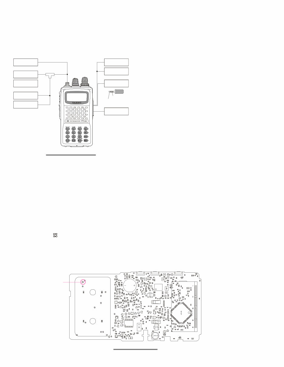
10 Alignment Test Setup Set up the test equipment as shown below for transceiver alignment, and apply 9.9 V DC power to the transceiver. Refer to the drawings for Alignment Points. PLL Reference Frequency 1. Tune the frequency to 435.050 MHz, then set the trans- mit power level to “LOW.” 2. Press the [F/W] key, then press the [BAND(BAND DN)] key to set the alignment parameter to “A0 REF.xxx,” if needed. 3. With in five second of appearing the “A0 REF.xxx” on the display, press the PTT switch to activate the trans- mitter, adjust the DIAL knob so that the counter fre- quency reading is 435.050 MHz (±100 Hz). RF Front-end Tuning 1. Connect the DC voltmeter to TP1015 on the MAIN unit, then inject a 439.050 MHz signal at a level of +10 dBµ (with 1 kHz modulation @±3.5 kHz deviation) from the RF signal generator. 2. Tune the frequency to 439.050 MHz. 3. Press the [F/W] key, then press the [BAND(BAND DN)] key to set the alignment parameter to “A1 TUN.xxx.” 4. With in five second of appearing the “A1 TUN.xxx” on the display, adjust the DIAL knob so that the DC volt- meter reaches maximum deflection. The FT-60R’s RF Front-end has a broad bandwidth. Therefore, prior to adjustment you must adjust the DIAL knob to set the frequency to the middle of the band, in step 2, so you can set peak in the DC voltmeter’s deflection in the center of the RF passband. 5. Tune the frequency to 145.050 MHz. 6. Inject a 145.050 MHz signal at a level of +10 dBµ (with 1 kHz modulation @±3.5 kHz deviation) from the RF signal generator. 7. Press the [F/W] key to recall the alignment parameter to “A1 TUN.xxx.” 8. With in five second of appearing the “A1 TUN.xxx” on the display, adjust the DIAL knob so that the DC volt- meter reaches maximum deflection. As in the previ- ous section, be sure to set the DIAL knob for the center of the band prior to making this adjustment. Entering the Alignment Mode Alignment of the FT-60R is performed using a front pan- el software-based procedure. To perform alignment of the transceiver, it must first be placed in the “Alignment Mode,” in which the adjustments will be made and then stored into memory. To enter the Alignment mode: 1. Press and hold in the MONI and LAMP switches turn- ing the radio on. Once the radio is on, release these two switches. 2. Press the keypad in the following sequence: [(MHz)] [0( )SET] [1(SQ TYP)] [7(P1)] [V/M(PRI)] 3. Press the [F/W] key to cause “A0 REF.xxx” to appear on the display for five seconds, this signifies that the trans- ceiver is now in the “Alignment Mode.” MAIN UNIT TEST POINT TP1015 FT-60R ALIGNMENT SETUP 8-ohm AF Dummy Load RF Signal Generator SINAD Meter In-Line Wattmeter Deviation Meter 50-ohm RF Dummy Load Frequency Counter AF Signal Generator Regulated 9.9 VDC P.S. AF Signal Input AF Signal Output
Looking for detailed information on how to fix your device? Our service workshop repair manuals are the perfect solution for both professional mechanics and DIY enthusiasts. These manuals are model-specific and not generic, ensuring you have the exact information you need for your specific device.
By using these manuals, you can prevent yourself from being misled by unethical repairmen and fully understand the ins and outs of your device. The manual contains comprehensive information beneficial for every owner and user.
Upon completion of payment, the manual will be instantly available for download, eliminating the need to wait for unreliable postal delivery. Additionally, you have the flexibility to print only the pages you require, saving time and resources.