

Kenwood TS 850S Service manual
What's Included?
Fast Download Speeds
Online & Offline Access
Access PDF Contents & Bookmarks
Full Search Facility
Print one or all pages of your manual
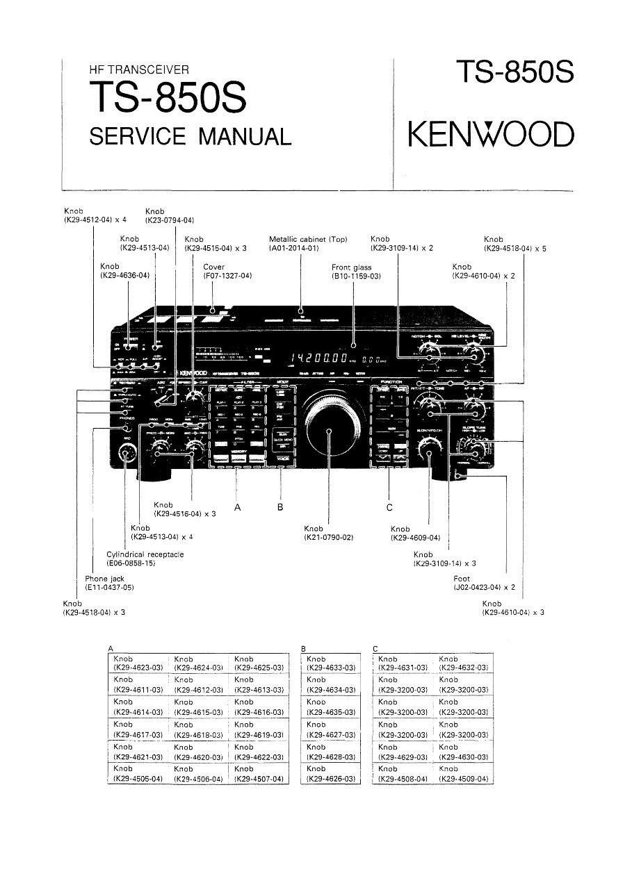
1
HF TRANSCEIVER
TS-8508
SERVICE MANUAL
Knob
(K29-4512-04) x 4
Knob
(K23-0794-04l
TS-8508
KENWOOD
Knob Knob
(K29-4513-04) (K29-4515-04) x 3
Metallic cabinet {Top)
(A01-2014-01)
Knob
(K29-3109-14) x 2
Knob
(K29-4518-04) x 5
Knob
(K29-4636-04)
Cover
{F07-1327-04)
Knob
(K29-4516-04) x 3
A B
Knob
(K29-4513-04l x 4
Cylindrical receptacle
(E06-0858-15)
Phone jack
(E11-0437-05)
Knob
(K29-4518-04) x 3
Knob
(K29-4507-04)
Front glass
(B 10-1159-03)
Knob
(K29-4610-04) x 2
Knob
(K21-0790-02)
B c
I Knob
I (K29-4633-03)
I
Knob
{K29-4634-03)
Knob
(K29-4635-03)
Knob
(K29-4627-03)
Knob
(K29-4628-03)
Knob
(K29-4626-03)
c
Knob
(K29-4609-04)
Knob
(K29-3109-14) x 3
Foot
(J02-0423-04) x 2
Knob Knob
Knob
(K29-3200-03l ,
Knob Knob
Knob
(K29-4610-04) x 3
(K29-3200-03) (K29-3200-03l
Knob Knob
(K29-4629-03) (K29-4630-03)
Knob Knob
2
TS-8508
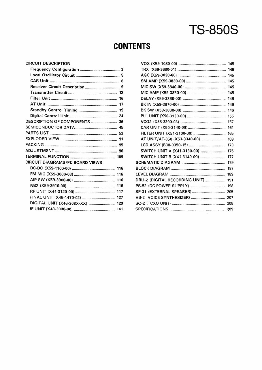
CONTENTS
CIRCUIT DESCRIPTION
Frequency Configuration .......•......................•......• 3
Local Oscillator Circuit ..............•..........•.......•.•...... 5
CAR Unit ...........................................................•.•.... 6
Receiver Circuit Description ................................. 9
Transmitter Circuit ............................................... 13
Filter Unit ............................................................... 16
AT Unit ................................................................... 17
Standby Control Timing ..................................... 19
Digital Control Unit .............................................. 24
DESCRIPTION OF COMPONENTS ......................... 36
SEMICONDUCTOR DATA ........................................ 45
PARTS LIST ................................................................ 53
EXPLODED VIEW ...................................................... 91
PACKING .................................................................... 95
ADJUSTMENT ........................................................... 96
TERMINAL FUNCTION........................................... 109
CIRCUIT DIAGRAMS/PC BOARD VIEWS
DC-DC (X59-1100-00) ......................................... 116
FM MIC (X59-3000-03) ....................................... 116
AIP SW (X59-3900-00) ....................................... 116
NB2 (X59-3910-00) ............................................. 116
RF UNIT (X44-3120-00) ................· ...................... 117
FINAL UNIT (X45-1470-02) ............................... 127
DIGITAL UNIT (X46-308X-XX) ......................... 129
IF UNIT {X48-3080-00) ....................................... 141
VOX (X59-1080-00) ............................................ 145
TRX (XS9-3680-01 ) . ... ... ............ ............. ............. 145
AGC (X59-3820-00) ............................................. 145
SM AMP (X59-3830-00) ..................................... 145
MIC SW (X59-3840-00) ...................................... 145
MIC AMP (X59-3850-00) .................................... 145
DELAY (X59-3860-00) ........................................ 146
BK IN (X59-3870-00) ........................................... 146
BK SW (X59-3880-00) ........................................ 146
PLL UNIT (XS0-3130-00) .................................... 155
VC02 (XSS-3390-03) ........................................... 157
CAR UNIT (XS0-3140-00) ................................... 161
FIL TEA UNIT (X51-3100-00) .............................. 165
AT UNIT/AT-850 (XSJ-3340-00) ....................... 169
LCD ASSY (B38-0350-15) .................................. 173
SWITCH UNIT A (X41-3130-00) ....................... 175
SWITCH UNIT B (X41-3140-00) ........................ 177
SCHEMATIC DIAGRAM ......................................... 179
BLOCK DIAGRAM ................................................... 187
LEVEL DIAGRAM .................................................... 189
DRU-2 (DIGITAL RECORDING UNIT) ................... 191
PS-52 (DC POWER SUPPLY) ................................. 198
SP-31 (EXTERNAL SPEAKER) ............................... 205
VS-2 (VOICE SYNTHESIZER) ................................ 207
S0-2 (TCXO UNIT) .................................................. 208
SPECIFICATIONS .................................................... 209
3
TS-8508
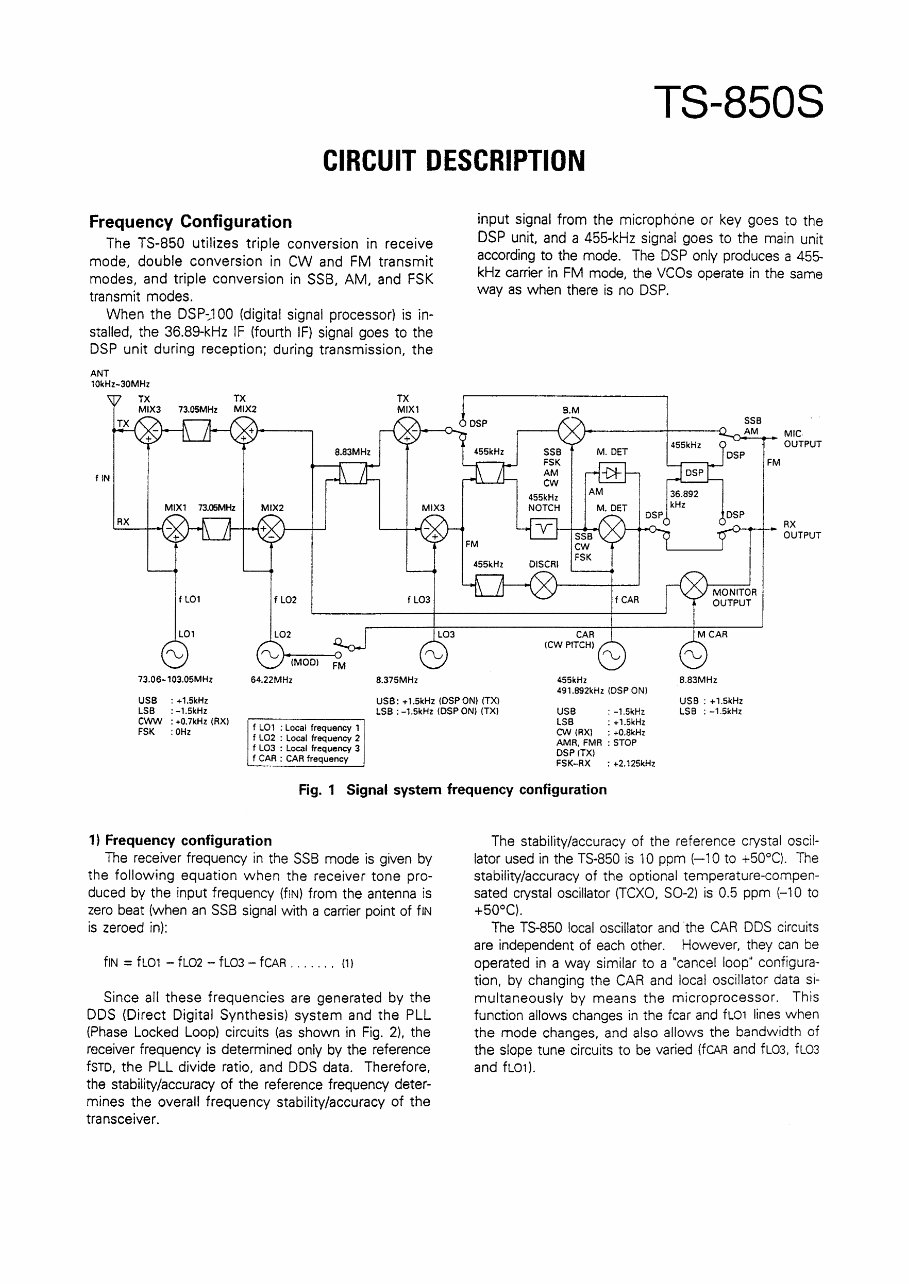
CIRCUIT DESCRIPTION
Frequency Configuration
The TS-850 utilizes triple conversion in receive
mode, double conversion in CW and FM transmit
modes, and triple conversion in SSS, AM, and FSK
transmit modes.
When the DSP-J 00 (digital signal processor) is in-
stalled, the 36.89-kHz IF (fourth IF) signal goes to the
DSP unit during reception; during transmission, the
ANT
10kHz-30MHz
TX TX
MIX3 73.0SMHz MIX2
flN
f LOl f L02 fl03
LOl
73.06-103.0SMHz 64.22MHz 8.375MHz
L03
input signal from the microphone or key goes to the
DSP unit, and a 455-kHz signal goes to the main unit
according to the mode. The DSP only produces a 455-
kHz carrier in FM mode, the VCOs operate in the same
way as when there is no DSP.
455kHz DISCRI
CAR
!CW PITCH)
455kHz
f CAR
491.892kHz (OSP ON)
OUTPUT
8.83MHz
USB : + 1.5kHz
LSB :-1.5kHz
USB: +1.SkHz (DSPON} (TX)
LSB: -1.SkHz (DSP ON} (TX) USB : -1.SkHz
USB : +1.SkHz
LSB : -1.SkHz
CWW : +0.7kHz (RX)
FSK : OHz
f L01 : Local frequency 1
f L02 : Local frequency 2
f L03 : Local frequency 3
f CAR : CAR frequency
LSB : +1.SkHz
CW (RX) : +O.SkHz
AMR. FMR : STOP
DSP (TX)
FSK-RX : +2.125kHz
Fig. 1 Signal system frequency configuration
1) Frequency configuration
The receiver frequency in the SSB mode is given by
the following equation when the receiver tone pro-
duced by the input frequency (flN) from the antenna is
zero beat (when an SSB signal with a carrier point of f1N
is zeroed in):
flN = f L01 -f L02 -f L03 -f CAR . . . . . . . (1)
Since all these frequencies are generated by the
DDS (Direct Digital Synthesis) system and the PLL
(Phase Locked Loop) circuits (as shown in Fig. 2), the
receiver frequency is determined only by the reference
fsTO, the PLL divide ratio, and DDS data. Therefore,
the stability/accuracy of the reference frequency deter-
mines the overall frequency stability/accuracy of the
transceiver.
The stability/accuracy of the reference crystal oscil-
lator used in the TS-850 is 10 ppm {-10 to +50°C). The
stability/accuracy of the optional temperature-compen-
sated crystal oscillator (TCXO, S0-2} is 0.5 ppm (-1 O to
+50°C).
The TS-850 local oscillator and 'the CAR DDS circuits
are independent of each other. However, they can be
operated in a way similar to a "cancel loop" configura-
tion, by changing the CAR and local oscillator data si-
multaneously by means the microprocessor. This
function allows changes in the fear and fL01 lines when
the mode changes, and also allows the bandwidth of
the slope tune circuits to be varied (fCAR and fL03, fL03
and fL01).
4
TS-8508
CIRCUIT DESCRIPTION
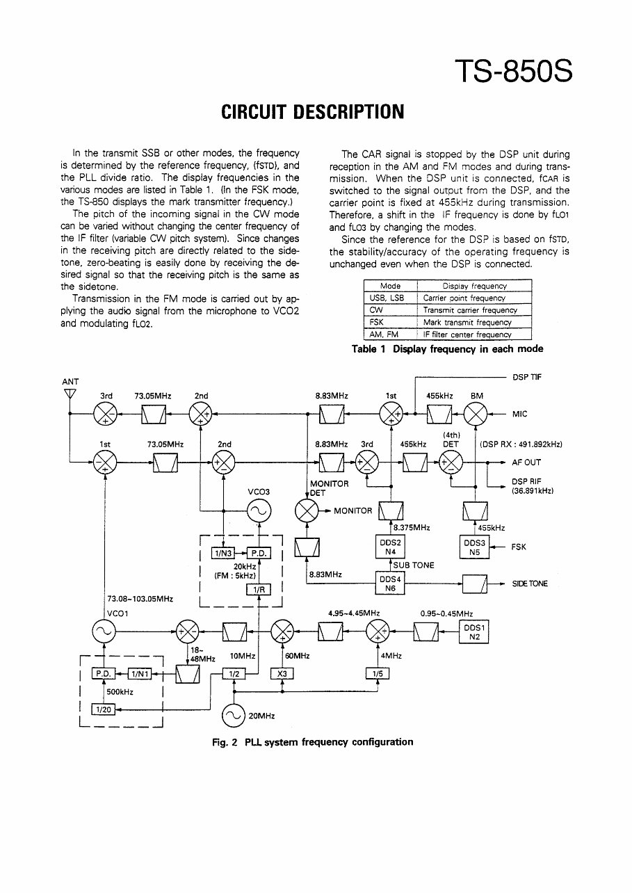
In the transmit SSS or other modes, the frequency
is determined by the reference frequency, {fSTD), and
the PLL divide ratio. The display frequencies in the
various modes are listed in Table 1. {In the FSK mode,
the TS-850 displays the mark transmitter frequency.)
The pitch of the incoming signal in the CW mode
can be varied without changing the center frequency of
the IF filter (variable CW pitch system). Since changes
in the receiving pitch are directly related to the side-
tone, zero-beating is easily done by receiving the de-
sired signal so that the receiving pitch is the same as
the sidetone.
Transmission in the FM mode is carried out by ap-
plying the audio signal from the microphone to VC02
and modulating fL02.
ANT
3rd 73.0SMHz 2nd
1st 73.0SMHz 2nd
VC03
73.08-103.0SMHz
The CAR signal is stopped by the DSP unit during
reception in the AM and FM modes and during trans-
mission. When the DSP unit is connected, fCAR is
switched to the signal output from the DSP, and the
carrier point is fixed at 455kHz during transmission.
Therefore, a shift in the IF frequency is done by fL01
and fL03 by changing the modes.
Since the reference for the DSP is based on fsm,
the stability/accuracy of the operating frequency is
unchanged even when the DSP is connected.
8.83MHz
Mode Display frequency
USS, LSB Carrier point frequency
cw Transmit carrier frequency
FSK Mark transmit frequency
AM. FM IF filter center frequency
Table 1 Display frequency in each mode
1st 455kHz
DSP TIF
BM
MIC
(OSP RX : 491.892kHz)
AF OUT
DSP RIF
(36.891 kHz)
FSK
SIDE TONE
Fig. 2 PLL system frequency configuration
5
TS-8508
CIRCUIT DESCRIPTION
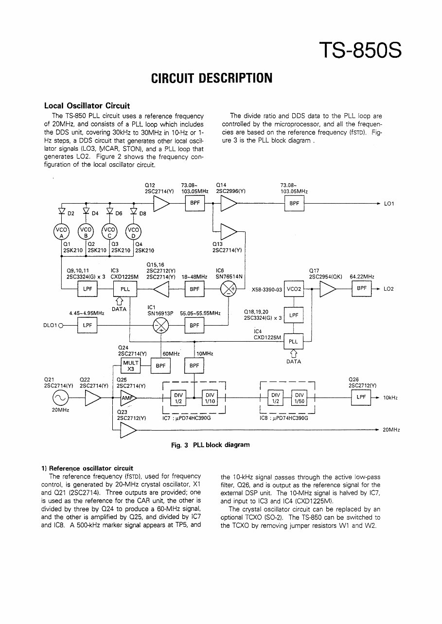
Local Oscillator Circuit
The TS-850 PLL circuit uses a reference frequency
of 20MHz, and consists of a PLL loop which includes
the DDS unit, covering 30kHz to 30MHz in 10-Hz or 1-
Hz steps, a DDS circuit that generates other local oscil-
lator signals (L03, (YlCAR, STON). and a PLL loop that
generates L02. Figure 2 shows the frequency con-
figuration of the local oscillator circuit.
The divide ratio and DDS data to the PLL loop are
controlled by the microprocessor, and all the frequen-
cies are based on the reference frequency (fSTD). Fig-
ure 3 is the PLL block diagram .
012 73.08- 014 73.08-
103.05MHz 2SC2714(Y} 103.05MHz 2SC2996(Y)
015,16
013
2SC2714(Y)
09,10,11 IC3 2SC2712(Y) IC6 017
2SC3324(G) x 3 CXD1225M 2SC2714(Y) 18-48MHz SN76514N 2SC2954(QKJ 64.22MHz
4.45-4.95MHz
DL01
20MHz
DATA
023
2SC2712(Y}
IC1
SN16913P 55.05-55.55MHz
IC7 : μPD74HC390G
018, 19,20
2SC3324(G) x 3
IC4
CXD1225M
DATA
ICS : μPD7 4HC390G
026
2SC2712(Y)
Fig. 3 PLL block diagram
1) Refererwe oscillator circuit
The reference frequency (fSTD), used for frequency
control, is generated by 20-MHz crystal oscillator, X1
and 021 {2SC2714). Three outputs are provided; one
is used as the reference for the CAR unit, the other is
divided by three by 024 to produce a 60-MHz signal,
and the other is amplified by 025, and divided by IC7
and IC8. A 500-kHz marker signal appears at TP5, and
the 10-kHz signal passes through the active low-pass
filter, 026, and is output as the reference signal for the
external DSP unit. The 10-MHz signal is halved by IC7,
and input to IC3 and IC4 (CXD1225M}.
The crystal oscillator circuit can be replaced by an
optional TCXO (S0-2). The TS-850 can be switched to
the TCXO by removing jumper resistors W1 and W2.
L01
L02
10kHz
20MHz
6
TS-8508
CIRCUIT DESCRIPTION
2)L02
01 (2SK508NV) of VC02 (X58-3390-03) is used to
generate a signal of 64.22MHz. The 10-MHz reference
frequency (fREF) is applied to pin 5 of IC4 (CXD1225M)
and is divided internally by 500 (2000 in FM mode), to
produce a 20-kHz (5-kHz in FM mode) comparison fre-
quency. The output from VC02 is applied to pin 11 of
IC4. and is divided internally by 3211 (12844 in FM
mode). It is then compared with the 20-kHz (5-kHz in
FM mode) reference signal by the phase comparator to
lock the VC02 frequency. Divide ratio data is supplied
by the digital unit.
The output is amplified to about 5dBm by amplifier
017 and passes through a low-pass filter. The imped
ance is converted and the signal is output.
3) L01 PLL loop
Four VCOs, 01 to 04 (2SK210 x 4), generate 73.08-
to 103.05-MHz signals. The reference signal of
1 OM Hz is applied to pin 5 of IC3 {CXD 1225M) and is di-
vided by 20 internally to produce a 500-kHz compari-
son frequency. The output signal passes through
amplifier 012 and a band-pass filter, and is divided into
two signals. One signal passes through the buffer and
low-pass filter of 014 (2SC2996) and is output to the
RF unit.
The other signal is applied to pin 5 of mixer IC6
(SN76514N). The DL01 signal of 4.45 to 4.95MHz is
input to pin 5 of mixer IC from the carrier unit, and a 60-
MHz signal (3 times the 20-MHz reference signal) is
input to pin 1. The signal of 55.05 to 55.55MHz signal
from mixer IC1 is applied to pin 11 of mixer IC6, and
becomes a signal of 18.03 to 48.0MHz. The signal is
output from pin 13, passes through the high-pass and
low-pass filters, amplifiers 016 (2SC2714) and 015
(2SC2712), and is applied to pin 11 of IC3 (CXD1225M).
This signal is divided by N 1 internally, compared
with a 500-kHz signal by the phase comparator. and
the mixer output frequency is locked in 500-kHz steps.
Divide ratio N 1 is sent from the digital unit as data (76
to 136) that covers 30kHz to 30MHz in 500-kHz steps.
One of the four VCOs is selected according to the VCO
switching data from the digital unit.
DLO 1 sweeps 4.45 to 4.95MHz in 10-Hz or 1-Hz
steps. The L01 output covers 73.08 to 103.05MHz in
10-Hz or 1-Hz steps, .3nd is output to the RF unit.
4) PLL data
The TS-850 has two PLLs as shown below, to which
the main microprocessor sends PLL data based on the
frequency indicated for each of the PLLs ..
· VFO PLL
· Local oscillator PLL for frequency conversion
The VCOs are selected depending upon conditions:
·Main encoder changes VC01
· Mode changes VC02
When each PLL IC outputs an unlock signal and one;
of the PLLs is unlocked, the display is changed to
• ..... • (decimal points only) to indicate that a PLL is
unlocked.
Unlocking of each PLL can be confirmed by the fact
that the status is output to the AO terminal of pin 8 of
the PLL IC (CXD1225M) as UL data.
Loop VCO No. i IC No. Comparison freq'/ Variable Frequency
Divide ratio divide ratio (MHz)
L01 VC01 I IC3 SOOk/20 36-96
73.08-103.0
L02 I VC02 j IC4
20k/500
I 3211 I
64.22
Sk/2000 (FM) 12844 (FM)
CAR Unit
The TS-850 CAR unit has four newly developed DDS
!Cs, and generates small PLL steps (DLO 1) that cover
1 OkHz to 30MHz in 1-Hz steps, the third local oscillator
{L03), CAR (CAR, MCAR), sidetone (STON), and sub-
carrier signals. Kenwood's original DDS IC frequency
modulation function is provided for FSK and subtone
modulation.
1) Reference signal
The 20-MHz reference signal from the PLL unit is
amplified by 03, buffered by CMOS inverter IC9, and
supplied to the DDS !Cs (IC1 to IC4) and IC5. This sig-
nal is halved by IC1 to IC4 to produce a DDS reference
signal. It is divided by 5 by ICS, and a 4-MHz signal is
supplied to the mixer that converts the IC1 output to
DL01.
2) DL01 generation
Digital signals from 0.95 to 0.45MHz are generated
by IC1, converted to analog signals by the digital-to-
analog (D/A) converter consisting of CP1, CP2. and 01,
passed through a low-pass filter, and are then applied
to mixer IC6. Here they are mixed with a 4-MHz signal
from IC5. The resulting signal is filtered by a combina-
tion of high-pass and low-pass filters to produce a sig-
nal in the range of 4.95 to 4.45MHz. This signal is out-
put from buffer 02 to the PLL unit as DLO 1.
7
TS-8508
CIRCUIT DESCRIPTION
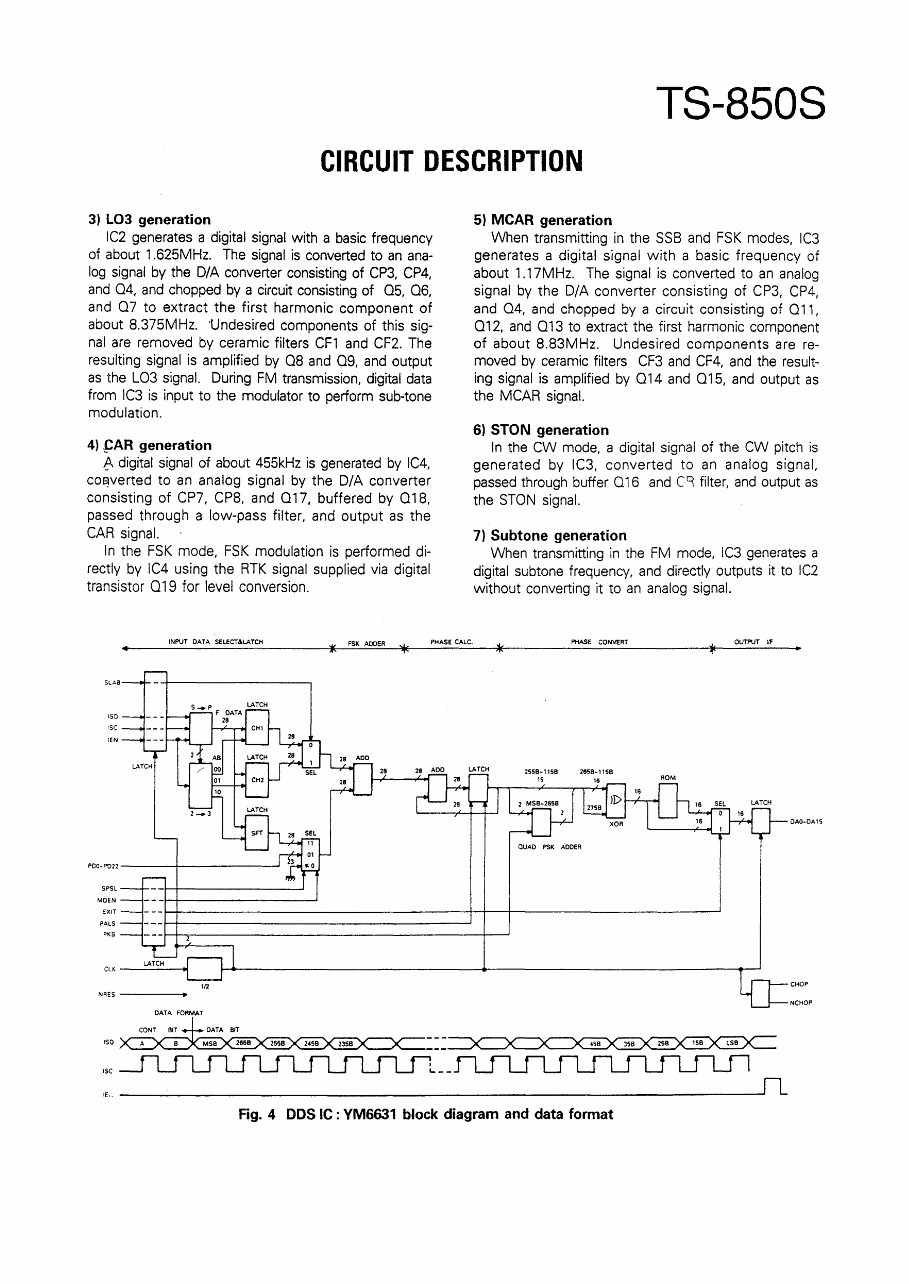
3) L03 generation
IC2 generates a digital signal with a basic frequency
of about 1.625MHz. The signal is converted to an ana-
log signal by the D/A converter consisting of CP3, CP4,
and 04, and chopped by a circuit consisting of 05, 06,
and 07 to extract the first harmonic component of
about 8.375MHz. ·undesired components of this sig-
nal are removed by ceramic filters CF1 and CF2. The
resulting signal is amplified by 08 and 09, and output
as the L03 signal. During FM transmission, digital data
from IC3 is input to the modulator to perform sub-tone
modulation.
4) generation
8 digital signal of about 455kHz is generated by IC4,
coa,verted to an analog signal by the D/A converter
consisting of CP7, CPS, and 017, buffered by 018,
passed through a low-pass filter, and output as the
CAR signal.
In the FSK mode, FSK modulation is performed di-
rectly by IC4 using the RTK signal supplied via digital
transistor 019 for level conversion.
INPUT DATA SELECT&LATCH
j( FSK ADDER *
112
NRES----
DATA FORMAT
ISO
ISC
PHASE CALC.
5) MCAR generation
When transmitting in the SSB and FSK modes, IC3
generates a digital signal with a basic frequency of
about 1.17MHz. The signal is converted to an analog
signal by the D/A converter consisting of CP3, CP4,
and 04, and chopped by a circuit consisting of 011,
012, and 013 to extract the first harmonic component
of about 8.83MHz. Undesired components are re-
moved by ceramic filters CF3 and CF4, and the result-
ing signal is amplified by 014 and 015, and output as
the MCAR signal.
6) STON generation
In the CW mode, a digital signal of the CW pitch is
generated by IC3, converted to an analog signal,
passed through buffer 016 and C9 filter, and output as
the STON signal.
7) Subtone generation
When transmitting in the FM mode, IC3 generates a
digital subtone frequency, and directly outputs it to IC2
without converting it to an analog signal.
PHASE CONVERT OUTPUT ti"
OAO-DA15
CHOP
NCH OP
1e,. ------------------'"'-----------------------'
Fig. 4 DDS IC : VM6631 block diagram and data format
8
TS-8508
CIRCUIT DESCRIPTION
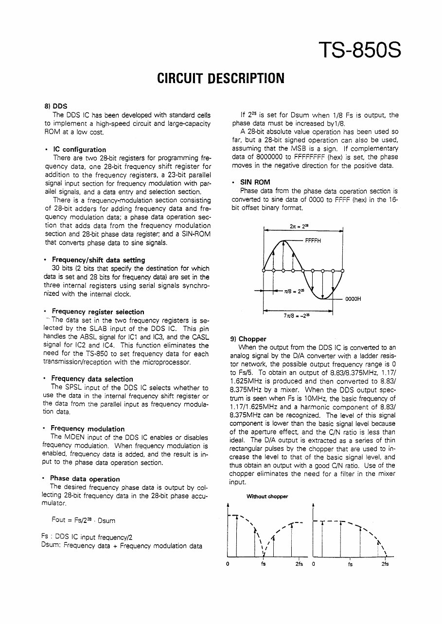
8) DDS
The DDS IC has been developed with standard cells
to implement a high-speed circuit and large-capacity
ROM at a low cost.
• IC configuration
There are two 28-bit registers for programming fre-
quency data, one 28-bit frequency shift register for
addition to the frequency registers, a 23-bit parallel
signal input section for frequency modulation with par-
allel signals, and a data entry and selection section.
There is a frequency-modulation section consisting
of 28-bit adders for adding frequency data and fre-
quency modulation data; a phase data operation sec-
tion that adds data from the frequency modulation
section and 28-bit phase data register; and a SIN-ROM
that converts phase data to sine signals.
• Frequency/shift data setting
30 bits (2 bits that specify the destination for which
data is set and 28 bits for frequency data) are set in the
three internal registers using serial signals synchro-
nized with the internal clock.
• Frequency register selection
data set in the two frequency registers is se-
lected by the SLAB input of the DDS IC. This pin
handles the ABSL signal for IC1 and IC3, and the CASL
signal for IC2 and IC4. This function eliminates the
need for the TS-850 to set frequency data for each
transmission/reception with the microprocessor.
• Frequency data selection
The SPSL input of the DDS IC selects whether to
use the data in the internal frequency shift register or
the data from the parallel input as frequency modula-
tion data.
• Frequency modulation
The MOEN input of the DDS IC enables or disables
frequency modulation. When frequency modulation is
enabled, frequency data is added, and the result is in-
put to the phase data operation section.
• Phase data operation
The desired frequency phase data is output by col-
lecting 28-bit frequency data in the 28-bit phase accu-
mulator.
Fout = Fs/2
28
. Dsum
Fs : DDS IC input frequency/2
Dsum: Frequency data + Frequency modulation data
0
If 2
25
is set for Dsum when 1 /8 Fs is output, the
phase data must be increased by1 /8.
A 28-bit absolute value operation has been used so
far, but a 28-bit signed operation can also be used,
assuming that the MSB is a sign. If complementary
data of 8000000 to FFFFFFFF (hex) is set, the phase
moves in the negative direction for the positive data.
• SIN ROM
Phase data from the phase data operation section is
converted to sine data of 0000 to FFFF (hex) in the 16-
bit offset binary format.
27t = 2
28
7rr./8 = -2
25
9) Chopper
When the output from the DDS IC is converted to an
analog signal by the D/A converter with a ladder resis-
tor network, the possible output frequency range is 0
to Fs/5. To obtain an output of 8.83/8.375MHz, 1.17/
1.625MHz is produced and then converted to 8.83/
8.375MHz by a mixer. When the DDS output spec-
trum is seen when Fs is 1 OM Hz, the basic frequency of
1.17/1.625MHz and a harmonic component of 8.83/
8.375MHz can be recognized. The level of this signal
component is lower than the basic signal level because
of the aperture effect, and the C/N ratio is less than
ideal. The D/A output is extracted as a series of thin
rectangular pulses by the chopper that are used to in-
crease the level to that of the basic signal level, and
thus obtain an output with a good C/N ratio. Use of the
chopper eliminates the need for a filter in the mixer
input.
Without chopper
......
'
- '
l',
.,,,.
\
/
\
I
\I \
\ \
fs 2fs 0 fs 2fs
9
TS-8508
CIRCUIT DESCRIPTION
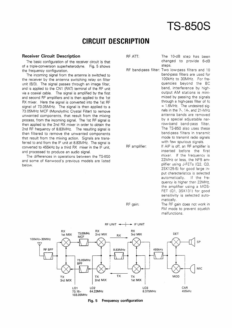
Receiver Circuit Description
The basic configuration of the receiver circuit is that
of a triple-conversion superheterodyne. Fig. 5 shows
the frequency configuration.
The incoming signal from the antenna is switched to
the receiver by the antenna switching relay on filter
unit (8/3). The signal passes through an image filter,
and is applied to the CN 1 (RA TI terminal of the RF unit
via a coaxial cable. The signal is amplified by the first
and second RF amplifiers and is then applied to the 1st
RX mixer. Here the signal is converted into the 1st RF
signal of 73.05MHz. The signal is then applied to a
73.05MHz MCF (Monolythic Crystal Filter) to remove
unwanted components, that result from the mixing
process, from the incoming signal. The 1st RF signal is
then applied to the 2nd RX mixer in order to obtain the
2nd RF frequency of 8.83MHz. The resulting signal is
then filtered to remove the unwanted components
that result from the mixing action. Signals are trans-
ferred to and from the IF unit at 8.83MHz. The signal is
converted to 455kHz by a third RX mixer in the IF unit,
and processed to produce an audio signal.
The differences in operations between the TS-850
and some of Kenwood's previous models are listed
below.
RF ATI: The 10-dB step has been
changed to provide 6-dB
steps.
RF band-pass filter: Two low-pass filters and 1O
band-pass filters are used for
1 OOkHz to 30MHz. For fre-
quencies beyond the BC
band, interference by high-
output AM stations is mini-
mized by passing the signals
through a high-pass filter of fc
= 1.6MHz. The undesired sig-
nals in the 7-, 14-, and 21-MHz
antenna bands are removed
by a special adjustable nar-
row-band band-pass filter.
The TS-850 also uses these
band-pass filters in transmit
mode to transmit radio signals
RF amplifier:
RF gain:
with few spurious signals.
If AIP is off, an RF amplifier is
inserted before the first
mixer. If the frequency is
22MHz or less, the NFB am-
plifier using J-FETs (02, 03,
2SK125-5) for good large in-
put characteristics is selected
automatically. If the fre-
quency is higher than 22M Hz,
the amplifier using a MOS-
FET (01, 3SK131) for good
sensitivity is selected auto-
matically.
The RF gain does not work in
FM mode to prevent squelch
malfunctions.
RF UNIT IF UNIT
RX
1st MIX
1OOkHz-30M Hz
RF BPF
TX
3rd MIX
RX
2nd MIX
TX
2nd MIX
L01 L02
73. 15- 64.22MHz
103.0SMHz
RX
8.83MHz
TX
RX
3rd MIX
TX
1st MIX
L03
8.375MHz
Fig. 5 Frequency configuration
DET
MOD
CAR
455kHz
SP
MIC
10
CIRCUIT DESCRIPTION
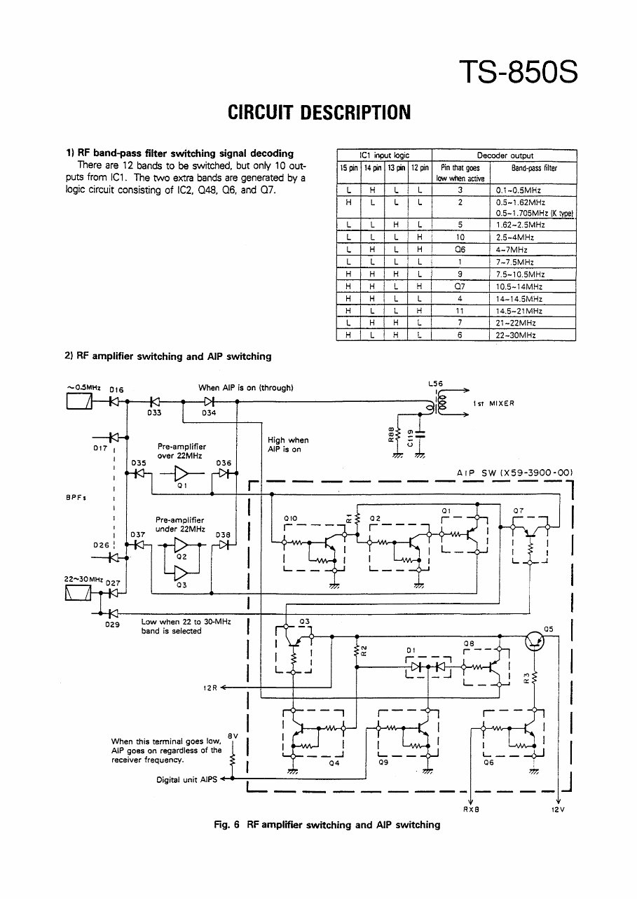
1) RF band-pass filter switching signal decoding
There are 12 bands to be switched, but only 10 out-
puts from IC1 . The two extra bands are generated by a
logic circuit consisting of IC2, 048, 06, and 07.
2) RF amplifier switching and AIP switching
Pre-amplifier
High when
017
AIP is on
over 22MHz
035
--t>--
036
r
-- QI
BPFs
IC1 input logic
15 pin 14 pin 13 pin
L H L
H L L
L L H
L L L
L H L
L L L
H H H
H H L
H H L
H L L
L H H
H L H
TS-8508
Decoder output
12 pin Pin that goes Band-pass filter
low when active
L 3 0.1-0.SMHz
L 2 0.5-1 .62MHz
0.5-1. 705MHz (K type}
L 5 1.62-2.SMHz
H 10 2.5-4MHz
H 06 4-7MHz
L 1 7-7.SMHz
L 9 7.5-10.SMHz
H 07 10.5-14MHz
L 4 14-14.5MHz
H 11 14.5-21MHz
L 7 21-22MHz
L 6 22-30MHz
A IP SW (X59-3900-00l
-----1
Pre-amplifier
.....
0::
under 22MHz
I Q7
029
037
$
038
03
Low when 22 to 30-MHz
band is selected
03
I
I
..J
t2R ----------
av
When this terminal goes low,
AIP goes on regardless of the
receiver frequency.
Digital unit AIPS
L
---,
I
__ _J
04
N
a::
Fig. 6 RF amplifier switching and AIP switching
as
r--
RXB
I
I
L
I
I
I
I
I
I
I
I
__ J
t2V
You're Reading a Preview
What's Included?
Fast Download Speeds
Online & Offline Access
Access PDF Contents & Bookmarks
Full Search Facility
Print one or all pages of your manual
$30.99
Viewed 71 Times Today


Secure transaction
What's Included?
Fast Download Speeds
Online & Offline Access
Access PDF Contents & Bookmarks
Full Search Facility
Print one or all pages of your manual
$30.99
The Kenwood TS 850S Service manual is a comprehensive resource for both professional mechanics and DIY enthusiasts. This manual, available in English, spans 219 pages and provides detailed technical information essential for car repair. Whether you're troubleshooting, performing maintenance, or undertaking repairs, this manual is an invaluable tool for ensuring the optimal performance of the Kenwood TS 850S. It is available in .PDF format, making it easily accessible for reference and use.


