

VERTEX YAESU VX-7R Repair Service Manual
What's Included?
Fast Download Speeds
Online & Offline Access
Access PDF Contents & Bookmarks
Full Search Facility
Print one or all pages of your manual
Specification ............................................................................................................................................ 2
Exploded View & Miscellaneous Parts ............................................................................................. 4
Block Diagram ........................................................................................................................................ 5
Interconnection Diagram ...................................................................................................................... 6
Circuit Description ................................................................................................................................ 7
Alignment .............................................................................................................................................. 11
Board Unit (Schematics, Layouts & Parts)
RF Unit ............................................................................................................................................................................. 19
AF Unit ............................................................................................................................................................................ 33
CNTL Unit ....................................................................................................................................................................... 45
VCO Unit ......................................................................................................................................................................... 59
©2003 VERTEX STANDARD CO., LTD. EH009M90B
Technical Supplement
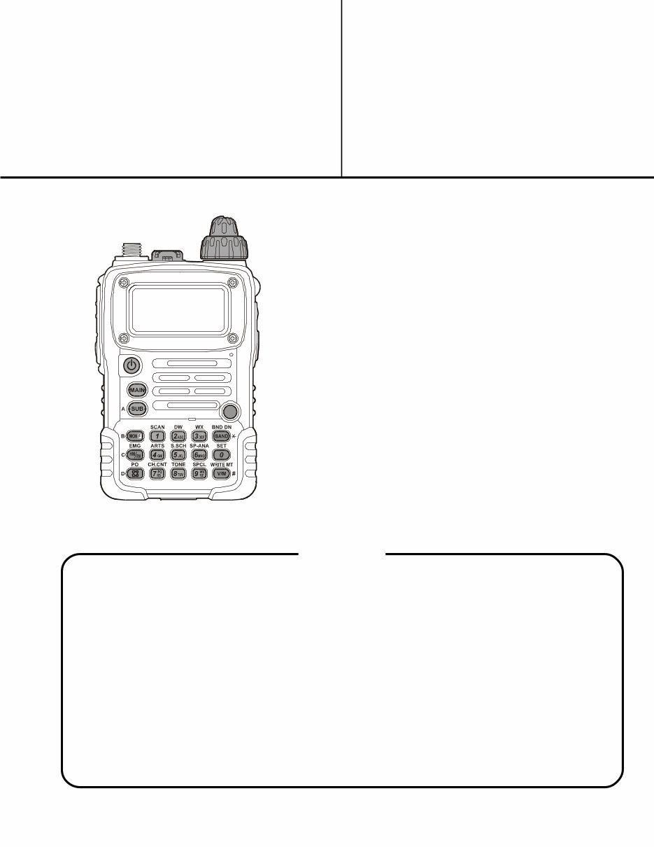
VX-7R
50/144/430 MHz Triple-Band
Heavy Duty Submersible Transceiver
Introduction
This manual provides the technical information necessary for servicing
the VX-7R 50/144/430 MHzTriple-Band Heavy Duty Submersible Trans-
ceiver.
Servicing this equipment requires expertise in handing surface-mount
chip components. Attempts by non-qualified persons to service this
equipment may result in permanent damage not covered by the war-
ranty, and may be illegal in some countries.
Two PCB layout diagrams provided for each double-sided board in
this transceiver. Each side of the board is referred to by the type of the
majority of components installed on that side ("Side A" or "Side B"). In
most cases one side has only chip components, and the other has either
a mixture of both chip and leaded components (trimmers, coils, electro-
lytic capacitors, ICs, etc.), or leaded components only.
While we believe the information in this manual to be correct, VER-
TEX STANDARD assumes no liability for damage that may occur as a
result of typographical or other errors that may be present. Your coop-
eration in pointing out any inconsistencies in the technical information
would be appreciated.
Contents
DW
VERTEX STANDARD CO., LTD.
4-8-8 Nakameguro, Meguro-Ku, Tokyo 153-8644, Japan
VERTEX STANDARD
US Headquarters
10900 Walker Street, Cypress, CA 90630, U.S.A.
YAESU EUROPE B.V.
P.O. Box 75525, 1118 ZN Schiphol, The Netherlands
YAESU UK LTD.
Unit 12, Sun Valley Business Park, Winnall Close
Winchester, Hampshire, SO23 0LB, U.K.
VERTEX STANDARD HK LTD.
Unit 5, 20/F., Seaview Centre, 139-141 Hoi Bun Road,
Kwun Tong, Kowloon, Hong Kong

2
Specifications
General
Frequency Ranges:
Channel Steps:
Frequency Stability:
Emission Type:
Antenna Impedance:
Supply Voltage:
Current Consumption:
Operating Temperature:
Case Size:
Weight:
Rx (MAIN):
0.5 - 1.8 MHz (BC Band)
1.8 - 30 MHz (SW Band)
30-59 MHz (50 MHz HAM: USA version)
30-76 MHz (50 MHz HAM: EXP version)
59-108 MHz (FM: USA version)
76-108 MHz (FM: EXP version)
108-137 MHz (Air Band)
137-174 MHz (144 MHz HAM)
174-222 MHz (VHF-TV)
222-225 MHz (220 MHz HAM: USA version)
225-420 MHz (ACT1: Action Band 1: USA version)
222-420 MHz (ACT1: Action Band 1: EXP version)
420-470 MHz (430 MHz HAM)
470-729 MHz (UHF-TV: USA version)
470-800 MHz (UHF-TV: EXP version)
800-999 MHz (ACT2: Action Band 2, cellular Blocked)
Rx (SUB):
50 - 54 MHz
137 - 174 MHz
420 - 470 MHz
Tx: 50 - 54 MHz (MAIN & SUB)
144 - 146 MHz or 144 - 148 MHz (MAIN & SUB)
222-225 MHz (MAIN, USA version)
430 - 440 MHz or 430 - 450 MHz (MAIN & SUB)
5/9/10/12.5/15/20/25/50/100 kHz
±5 ppm (+14°F to +122°F, –10°C to +50°C)
F2, F3, A3
50-ohm
Nominal: 7.4 V DC, Negative Ground
Operating: 10 - 16 V DC, Negative Ground (EXT DC jack)
150 mA (Mono Band Receive)
200 mA (Dual Band Receive)
55 mA (Mono Band Receive, Standby, Saver Off)
100 mA (Dual Band Receive, Standby, Saver Off)
25 mA (Mono Band Receive, Standby, Saver On "Save Ratio 1:5")
50 mA (Dual Band Receive, Standby, Saver On "Save Ratio 1:5")
400 µA (Auto Power Off)
1.6/1.3/1.0/0.7 A (50 MHz, Tx HI/L3/L2/L1)
1.71.4/1.1/0.8 A (144 MHz, Tx HI/L3/L2/L1)
0.6 A (220 MHz, Tx)
1.8/1.5/1.2/0.9/ A (430 MHz, Tx HI/L3/L2/L1)
–4°F to +140°F (–20°C to +60°C)
60 (W) x 90 (H) x 28 (D) mm (w/o knob & antenna)
250 g

3
Specifications are subject to change without notice, and are guaranteed within amateur bands only.
Specifications
Transmitter
RF Power Output:
Modulation Type:
Maximum Deviation:
Spurious Emission:
Microphone Impedance:
Receiver
Circuit Type:
Intermediate Frequencies:
Sensitivity:
Selectivity:
AF Output:
5/2.5/1.0/0.5 W (50/144/430 MHz, FM)
0.3 W (220 MHz, FM)
1.0 W (50 MHz, FM)
FM: Variable Reactance
AM: Early Stage (Low Level)
±5/±2.5 kHz
At least 60 dB below (@ Tx 1W)
2 k-ohm
N-FM, AM: Double-Conversion Superheterodyne
W-FM: Triple-Conversion Superheterodyne
1st: 47.25 MHz (N-FM, AM)
45.8 MHz (W-FM)
2nd: 450 kHz (N-FM, AM)
10.7 MHz (W-FM)
3rd: 1 MHz (W-FM)
3.0 µV for 10 dB SINAD (0.5 - 30 MHz, AM)
0.5 µV for 12 dB SINAD (30 - 50 MHz, N-FM)
0.16 µV for 12 dB SINAD (50 - 54 MHz, N-FM)
15 kHz/35 kHz (-6 dB/-60 dB: N-FM, AM)
200 kHz/300 kHz (-6 dB/-20 dB: W-FM)
200 mW @ 8 ohm for 10 % THD (@ 7.4V DC)
400 mW @ 8 ohm for 10 % THD (@ 13.8V DC)
4
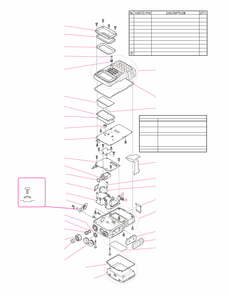
Exploded View & Miscellaneous Parts
SUPPLIED ACCESSORIES
VXSTD P/N DISCRIPTION
Q3000183 YHA-64
(depending on transceiver version)
Q3000185 YHA-65
Q8101014 YHA-63 50MHZ ADAPTER L
Q8101015 YHA-63 440MHZ ADAPTER S
Q9000786 LI-ION BATTERY FNB-80LI
Q9500087 NC-72A
Q9500088 NC-72B
(depending on transceiver version)
Q9500089 NC-72C
Q9500090 NC-72U
RA029630A BELT CLIP
S6000335 HAND STRAP
➀
➀
➁
➁
➁
➁
➃
➄
➂
➂
➂
➂
RA0400000
RUBBER PACKING
RA0417100
PANEL FRAME
RA0399500
WINDOW
RA0399400
DOUBLE FACE TAPE
RA0401600
O RING
RA0399800
LIGHT GUIDE (LED)
RA0400100
RUBBER KNOB (PTT)
RA0140100
MASK SHEET
RA0399700
HOLDER (PTT)
CP7342003 (SILVER)
CP7342005 (BLACK)
REAR CASE ASS’Y
with SMA CONNECTOR ASS’Y,
TERMINAL BOARD ASS’Y,
RUBBER HOLDER (PTT),
RUBBER KNOB (PTT)
RA01403AA
LATCH NAIL
FNB-80LI
RA0399900
REFLECTOR SHEET
RA014250A
DOUBLE FACE TAPE (LCD)
RA0399100
LIGHT GUIDE (LED)
Q7000426
LCD MODULE
RA0405600
MIC HOLDER RUBBER
CNTL-Unit
RA0426800
O RING
AF-Unit
RA0400900
O RING
RA0400200
STUD (X4 pcs)
RA0426900
O RING
RA0087900
SPECIAL NUT
CP7346002 (USA, SILVER)
CP7346003 (EXPORT, SILVER)
CP7346004 (GERMANY, SILVER)
CP7346006 (USA, BLACK)
CP7346007 (EXPORT, BLACK)
CP7346008 (GERMANY, BLACK)
PANEL ASS’Y
with RUBBER KNOB, MIC SHEET,
SP SHEET, SP, PROTECTOR L,
PROTECTOR R
➅
➆
➆
➇
➇
➆
➆
➆
➆
RA0292200
SPECIAL NUT
➈
➈
➈
➈
➉
➉
RA0400500
EXT CAP
RA0401200
ENCODER KNOB
RA0401900
VOLUME KNOB
RA0400600
CAP(SP/MIC)
RA0141600
RUBBER PACKING
There is a direction in
WASHER.
WASHER
SCREW
EXP CAP
FR008330C
FPC CABLE
➀ U9900137 BINDING HEAD SCREW M2X21.7 (W/ O RING) 2
➁ U9900138 BINDING HEAD SCREW M2X5 (W/ O RING) 4
➂ U07225120 PAN HEAD SCREW M2X2.5SUS#1 4
➃ U9900136 SPECIAL SCREW M2X2.35 1
➄ RA0304300 WASHER 1
➅ U00103002 PAN HEAD SCREW M2X3NI 1
➆ U00104002 PAN HEAD SCREW M2X4NI 6
➇ U9900140 TAPTITE SCREW M2X6SUS#3 2
➈ U44104002 TAPTITE SCREW M2X4NI 4
➉ U9900141 TAPTITE SCREW M1.7X5NI#3 2
U07125102 TAPTITE SCREW M1.7X2.5SUS#1 2
P0091335
CONNECTOR (EXT DC)
RF-Unit
P1091150
CONNECTOR (MIC/SP)
5
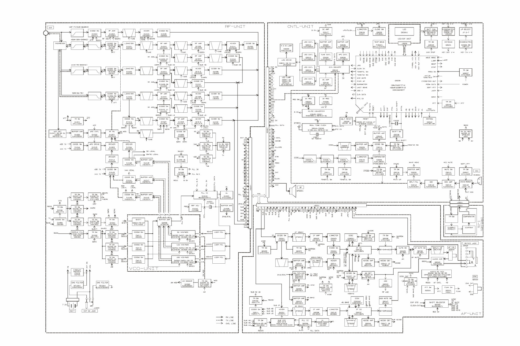
Block Diagram
6
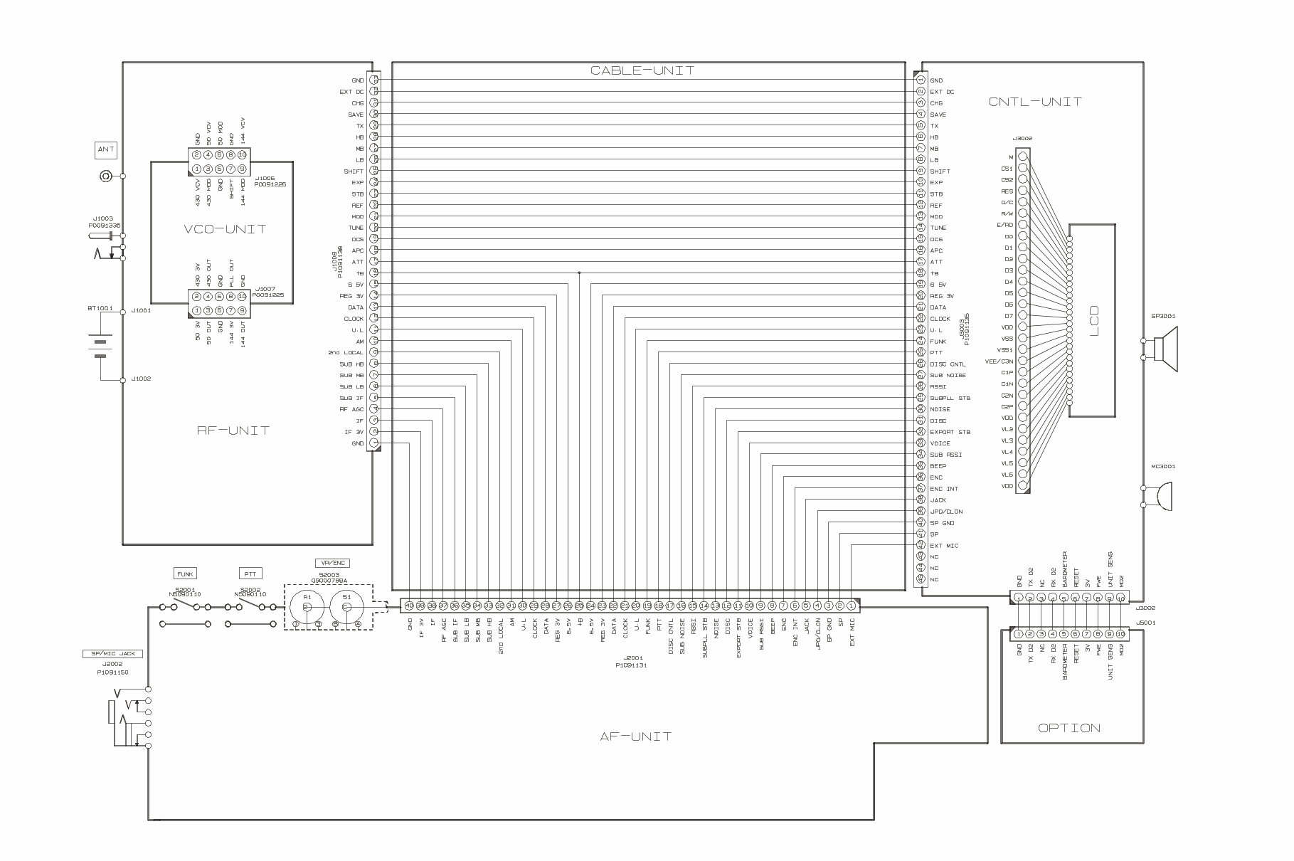
Interconnection Diagram

7
Circuit Description
The VX-7R consists of a RF-UNIT, a CNTL-UNIT and
an AF-UNIT. The RF-UNIT contains the receiver front end,
PLL IC, power and switching circuits, and the VCO-UNIT
for transmit and receive local signal oscillation. The CNTL-
UNIT contains the CPU, and audio ICs, and the power
circuitry for the LCD. The AF-UNIT contains the IF, and
audio ICs.
Receiver Signal Flow
The VX-7R includes five receiver front ends, each op-
timized for a particular frequency range and mode com-
bination.
(1) Triplexer
Signals between 0.5 and 540 MHz received at the an-
tenna terminal pass through a first low-pass filter com-
posed of C1266, C1269, C1289, C1291, C1296, C1297,
L1059, L1060, L1067 and L1068.
Received 430-MHz signals, after passing through the
low-pass filter, are fed to the UHF T/R switch circuit com-
posed of diode switch D1048 (RLS135), D1051 (1SV307).
Received 145-MHz signals, after passing through the
low-pass filter, are fed to the VHF T/R switch circuit com-
posed of diode switch D1053 (RLS135), D1054 (1SV307).
Received 50-MHz signals, after passing through the low-
pass filter, are fed to the 50MHz T/R switch circuit com-
posed of diode switch D1058 (RLS135), D1059 (1SV307).
(2) 145-MHz Band and 76-300MHz Reception
Received signals between 76 and 300 MHz pass through
the Triplexer circuit, low-pass filter/high-pass filter cir-
cuit, VHF T/R switch circuit and protector diode D1002
(1SS362) before additional filtering by a band-pass filter
prior to application to RF amplifier Q1004 (2SC5555). The
amplified RF signal is passed through a band-pass filter
to first mixer Q1012 (2SC5555). Meanwhile, VHF output
from the VCO-UNIT is amplified by Q1017 (2SC5374)
and applied through diode T/R switch D1041 (DAN222)
to mixer Q1012 as the first local signal.
The 47.25-MHz intermediate frequency product of the
mixer is delivered to the AF-UNIT.
The TUNE voltage from the CPU on the CNTL-UNIT is
amplified by DC amplifier Q3017 (NJU7007F2) and ap-
plied to varactors D1020 and D1022 (HVC369B), D1019,
D1021, D1023, D1024, D1033 and D1036 (1SV325) in the
variable frequency band-pass filters. By changing the elec-
trostatic capacitance of the varactors, optimum filter char-
acteristics are provided for each specific operating fre-
quency.
(3) 435-MHz Band and 222-540MHz Reception
Received signals between 222 and 540 MHz pass
through the Triplexer circuit, low-pass filter/high-pass
filter circuit, UHF T/R switch circuit and protector diode
D1001 (1SS362) before additional filtering by a band-pass
filter prior to application to RF amplifier Q1003
(2SC5555). The amplified RF signal is passed through a
band-pass filter, RF amplifier Q1006 (2SC5555) and band-
pass filter to first mixer Q1011 (2SC5555). Meanwhile,
UHF output from the VCO-UNIT is amplified by Q1016
(2SC5374) and applied through diode T/R switch D1045
(HN2D01FU) to mixer Q1011 as the first local signal.
The 47.25-MHz intermediate frequency product of the
mixer is delivered to the AF-UNIT.
The TUNE voltage from the CPU on the CNTL-UNIT is
amplified by DC amplifier Q3017 and applied to varac-
tors D1005, D1018, D1030 and D1031 (HVC358B) in the
variable frequency band-pass filters. By changing the elec-
trostatic capacitance of the varactors, optimum filter char-
acteristics are provided for each specific operating fre-
quency.
(4) 50-MHz-Band and 30-76 MHz Reception
Received signals between 30 and 76 MHz pass through
the Triplexer circuit, low-pass filter circuit, 50 MHz T/R
switch circuit and protector diode D1003 (1SS362) be-
fore additional filtering by a band-pass filter prior to ap-
plication to RF amplifier Q1005 (2SC5555). The ampli-
fied RF signal is passed through a band-pass filter to first
mixer Q1008 (2SC5555). Meanwhile, 50 MHz output from
the VCO-UNIT is amplified by Q1018 (2SC5374) and
applied through diode T/R switch D1046 (HN2D01FU) to
mixer Q1008 as the first local signal.
The 47.25-MHz intermediate frequency product of the
mixer is delivered to the AF-UNIT.
The TUNE voltage from the CPU on the CNTL-UNIT is
amplified by DC amplifier Q3017 and applied to varac-
tors D1025 and D1026 (1SV325) in the variable frequen-
cy band-pass filters. By changing the electrostatic capaci-
tance of the varactors, optimum filter characteristics are
provided for each specific operating frequency.
(5) 0.5 - 30 MHz Reception
Received signals between 0.5 and 30 MHz pass through
the Triplexer circuit, low-pass filter circuit, HF T/R switch
circuit and protector diode D1003 before additional fil-
tering by a band-pass filter prior to application to RF
amplifier Q1009 (2SC4915-0). The amplified RF signal is

8
Circuit Description
passed through a band-pass filter to first mixer Q1013
(2SC4915-0). Meanwhile, HF output from the VCO-UNIT
is amplified by Q1018 and applied through diode T/R
switch D1046 to mixer Q1013 as the first local signal.
The 47.25-MHz intermediate frequency product of the
mixer is delivered to the AF-UNIT.
The TUNE voltage from the CPU on the CNTL-UNIT is
amplified by DC amplifier Q3017 and applied to varac-
tors D1013 (HVR100) in the variable frequency band-pass
filters. By changing the electrostatic capacitance of the
varactors, optimum filter characteristics are provided for
each specific operating frequency.
(6) 540 - 999 MHz Reception
Received signals between 540 and 999 MHz pass
through the high-pass filter circuit, T/R switch D1004
(1SV271) prior to application to RF amplifier Q1002
(2SC5277). The amplified RF signal is passed through a
band-pass filter to first mixer Q1010 (2SC5277). Mean-
while, UHF output from the VCO-UNIT is amplified by
Q1016 and applied through diode T/R switch D1045 to
mixer Q1010 as the first local signal.
The 47.25-MHz intermediate frequency product of the
mixer is delivered to the AF-UNIT.
The TUNE voltage from the CPU on the CNTL-UNIT is
amplified by DC amplifier Q3017 and applied to varac-
tors D1015 and D1017 (HVC355B) in the variable frequen-
cy band-pass filters. By changing the electrostatic capaci-
tance of the varactors, optimum filter characteristics are
provided for each specific operating frequency.
(7) 47.25-MHz First Intermediate Frequency
The 47.25-MHz first intermediate frequency from the
first mixers is delivered from the RF-UNIT to the AF-UNIT
through jacks J1008 and J2001. On the AF-UNIT, the IF
for AM and FM-narrow signals is passed through NAR/
WIDE switch D2001 (DAP222) and the 47.25-MHz mono-
lithic crystal filter (MCF) XF2001 to narrow IF amplifier
Q2002 (2SC4915-0) for input to pin 16 of the Narrow IF
IC Q2016 (TA31136FN), after amplitude limiting by D2003
(DA221).
Meanwhile, a portion of the output of 11.7-MHz crystal
X1001 on the RF-UNIT is multiplied fourfold by Q2004
(2SC4915-0) and Q2012 (2SC4154E) to provide the 46.8-
MHz second local signal, applied to the Narrow IF IC.
Within the IC, this signal is mixed with the 47.25-MHz
first intermediate frequency signal to produce the 450 kHz
second intermediate frequency.
This second IF is filtered by ceramic filter CF2002
(ALFYM450F=k) and amplified by the limiting amplifier
within the Narrow IF IC before quadrature detection by
ceramic discriminator CD2001 (CDBM450C7).
Demodulated audio is passed from pin 9 of the Narrow
IF IC through the "Mute" analog switch Q2029 (2SJ364)
and squelch gate Q2036 (2SJ364) before de-emphasis at
Q2028 (DTC144EE).
The resulting audio is amplified by AF amplifier Q2040
(TDA7233D) and fed through the MIC/EAR jack J2002 to
internal speaker SP1001 or an external earphone.
(8) Squelch Control
Signal components in the neighborhood of 15 kHz con-
tained in the discriminator output pass through an active
band-pass filter composed of R2059, R2060, R2062, C2076,
C2078 and the operational amplifier between pins 7 and
8 within Narrow IF IC Q2016. They are then rectified by
D2012 and D2013 (MC2850) to obtain a DC voltage cor-
responding to the level of noise. This voltage is fed to pin
49 of CPU Q3035 (HD6472237TF10), which compares the
input voltage with a previously set threshold. When the
input voltage drops below the threshold, normally due to
the presence of a carrier, the CPU turns on squelch gate
Q2036 and allows any demodulated audio to pass. At the
same time, Q3001 and/or Q3003 and/or Q3004 goes on,
causing the BUSY/TX lamp D3033 (FRGB1312CE-10-TF)
to light.
Transmitter Signal Flow
(1) 145-MHz-Band Transmit/Receive Switching
Closing PTT switch S2002 on the AF-UNIT pulls the base
of Q3008 (DTA144EE) low, causing the collector to go
high. This signal is fed to pin 33 (PTT) of CPU Q3035,
allowing the CPU to recognize that the PTT switch has
been pushed. When the CPU detects closure of the PTT
switch, pin 10 (TX) goes high. This control signal is deliv-
ered to the RF-UNIT, where it switches Q1044 (UMW1)
and Q1043 (CPH6102) to produce the TX control signal
that activates Q1046 (2SA1774). At the same time, PLL
division data is fed to PLL IC Q1019 (MB15A01PFV1)
from the CPU, to disable the receiver power saver. Also,
it switches Q1048 (KRC654U) to disable the receiver cir-
cuits. This causes the "red" mode of BUSY/TX lamp D3033
to light.

9
Circuit Description
(2) Modulation
Voice signal input from either built-in microphone
MC3001 (EM-140) on the CNTL-UNIT or external jack
J2002 on the AF-UNIT is pre-emphasized by C3012 and
R3031, and processed by microphone amplifier Q3018
(NJM3403AV), IDC (instantaneous deviation control) cir-
cuit Q1014 to prevent overmodulation, and fed through
active low-pass filter Q1014.
During CTCSS operation, the voice signal is mixed with
the TONE ENC subaudible tone signal from pin 43 of the
CPU and delivered to the RF-UNIT through jacks J3003
and J1008. During DTMF operation, the DTMF tones from
pin 44 of the CPU are fed to the IDC stage.
(3) 145-MHz-Band Transmission
Modulating audio from the CNTL-UNIT passes through
deviation setting D/A converter Q3012 to the VHF modu-
lator portion of the VCO-UNIT mounted on the RF-UNIT.
This signal is applied to varactor D4005 (HSC277) in the
tank circuit of VHF VCO Q4004 (EC3H07B), which oscil-
lates at the desired VHF transmitting frequency. The
modulated VCO signal is buffered by amplifier Q4006
(EC3H07B) and Q1017 and delivered through VHF T/R
diode switch D1041 to the RF-UNIT. The modulated low-
level VHF transmit signal from the VCO is passed through
diode switch D1043 ( DAN222 ) to amplifier Q1014
(2SC5226-5). The modulated VHF transmit signal from
the VCO is amplified by Q1023 (2SK3475) and RF power
amplifier Q1027 (2SK3476) up to 0.05, 1.0, 2.5 or 5 Watts
(depending on the power source). The RF output passes
through TX diode switch D1053. RF output is passed by
the T/R switch and low-pass filter to suppress harmonics
and spurious products before output gets to the antenna
at the antenna terminal.
(4) 435-MHz-Band Transmission
Modulating audio from the CNTL-UNIT passes through
deviation setting D/A converter Q3012 to the UHF mod-
ulator portion of the VCO-UNIT mounted on the RF-
UNIT. This signal is applied to varactor D4002 (HSC277)
in the tank circuit of UHF VCO Q4002 (EC3H07B), which
oscillates at the desired UHF transmitting frequency. The
modulated VCO signal is buffered by amplifier Q4006 and
Q1016 and delivered through UHF T/R diode switch
D1045 to the RF-UNIT. The modulated low-level UHF
transmit signal from the VCO is passed through diode
switch D1045 (HN2D01FU) to amplifier Q1014. The mod-
ulated UHF transmit signal from the VCO is amplified
by Q1023 and RF power amplifier Q1027 up to 0.05, 1.0,
2.5 or 5 Watts (depending on the power source). The RF
output passes through TX diode switch D1048. RF out-
put is passed through the T/R switch and low-pass filter
to suppress harmonics and spurious products before out-
put gets to the antenna at the antenna terminal.
(5) 50-MHz-Band Transmission
Modulating audio from the CNTL-UNIT passes through
deviation setting D/A converter Q3012 to the 50 MHz
modulator portion of the VCO-UNIT mounted on the RF-
UNIT. This signal is applied to varactor D4009 (HSC277)
in the tank circuit of 50 MHz VCO Q4005 (EC3H07B),
which oscillates at the desired 50 MHz transmitting fre-
quency. The modulated VCO signal is buffered by ampli-
fier Q4006 and Q1018 and delivered through 50 MHz T/R
diode switch D1046 to the RF-UNIT. The modulated low-
level 50 MHz transmit signal from the VCO is passed
through diode switch D1046 (HN2D01FU) to amplifier
Q1014. The modulated 50 MHz transmit signal from the
VCO is amplified by Q1023 and RF power amplifier Q1027
up to 0.05, 1.0, 2.5 or 5 Watts (depending on the power
source). The RF output passes through TX diode switch
D1058. RF output is passed through the T/R switch and
low-pass filter to suppress harmonics and spurious prod-
ucts before output gets to the antenna at the antenna ter-
minal.

10
Circuit Description
PLL Frequency Synthesizer
PLL IC Q1019 on the RF-UNIT consists of a data shift
register, reference frequency divider, phase comparator,
charge pump, "intermittent operation" circuit, and band
selector switch. Serial PLL data from the CPU is convert-
ed into parallel data by the shift register in the PLL IC
and is latched into the comparative frequency divider and
reference frequency divider to set a frequency dividing
ratio for each. An 11.7-MHz reference signal produced
by X1001 is fed to "REF" pin 1 of the PLL IC. The internal
reference frequency divider divides the 11.7-MHz refer-
ence by 2,050 (or 1,640) to obtain a reference frequency of
5 kHz (or 6.25 kHz), which is applied to the phase com-
parator. Meanwhile, a sample of the output of VHF VCO
Q4004 or UHF VCO Q4002 or 50 MHz VCO Q4005 on the
VCO-UNIT, buffered by Q4006, is fed to the PLL IC, where
it is divided by the internal comparative frequency divid-
er to produce a comparative frequency which also is ap-
plied to the phase comparator. The phase comparator com-
pares the phase between the reference frequency and com-
parative frequency to output a pulse corresponding to the
phase difference between them. This pulse is fed to the
charge pump, and the output from the charge pump pass-
es through a loop filter composed of L1044, R1089, C1175,
and either R1090, C1192, R1103 and C1195 for VHF, or
R1086, C1189, R1102 and C1194 for UHF, or R1091, C1193,
R1104 and C1196 for 50 MHz, which convert the pulse
into a corresponding smoothed varactor control voltage
(VCV). The VCV is applied to varactors D4004 and D4013
(1SV325) in the VHF VCO tank circuit, or to varactor
D4001 (HVC355B) in the UHF VCO tank circuit, or to
varactors D4007 and D4008 (1SV325) in the 50 MHz VCO,
to eliminate any phase difference between the reference
frequency and comparative frequency, thus locking the
VCO oscillation frequency to the reference crystal. The
VCO frequency is determined by the frequency-dividing
ratio sent from the CPU to the PLL IC. During receiver
power save operation, the PLL circuit operates intermit-
tently to reduce current consumption, for which the "in-
termittent operation" control circuit reduces the lock-up
time.
You're Reading a Preview
What's Included?
Fast Download Speeds
Online & Offline Access
Access PDF Contents & Bookmarks
Full Search Facility
Print one or all pages of your manual
$30.99
Viewed 49 Times Today


Secure transaction
What's Included?
Fast Download Speeds
Online & Offline Access
Access PDF Contents & Bookmarks
Full Search Facility
Print one or all pages of your manual
$30.99
This manual includes a variety of technical information such as schematic diagrams, block diagrams, exploded views, alignment procedures, and board layouts. It provides a small preview of the schematic diagram for reference.
The manual features bookmarks for easy navigation and can be printed. It is compatible with both Windows and Mac operating systems.
Details:
- Pages: 64
- Language: English
- Publication ID: EH009M90B
- Publication Year: 2003
Contents:
- Specifications
- Exploded Views
- Block Diagrams
- Circuit Description
- Parts List
- Alignment Procedures
- Board/Parts Layouts
- Schematic Diagrams
This manual is for the Vertex-Yaesu VX-7R and is available in .PDF format.


